Electrical
1/42
Earn XP
Description and Tags
A6, LT 1-7
Name | Mastery | Learn | Test | Matching | Spaced |
|---|
No study sessions yet.
43 Terms
Semiconductors
Have exactly 4 valence electrons.
Doping
The injection of impurities into semiconductors to produce either N-type or P-type semiconductor materials.
N-type
Formed when a pentavalent impurity having 5 valence electrons is introduced into the pure semiconductor crystal.
Leaves the crystal with a surplus of electrons, or negative charge carriers.
Forms the cathode side of the diode.
P-type
Formed when a trivalent impurity having 3 valence electrons is introduced into the pure semiconductor crystal.
Leaves the crystal with an absence of electrons (or a hole), considered positive.
Forms the anode side of the diode.
Negative temperature coefficient
As the temperature increases, the resistance decreases, that is conductivity increases.
Heat sink
Diodes are commonly mounted on these to improve the dissipation of heat.
Barrier potential
Some of the free electrons in the N-type material combine with the holes of the P-type material
The P-type material gains some electrons (negative charge), and the N-type material loses some electrons (positive charge).
Reverse bias
Voltage applied so the cathode is more positive than the anode. Barrier potential is strengthened:
Free electrons in the N-type material are attracted toward the positive side of the applied potential.
The holes in the P-type are attracted toward the negative side of the applied potential.
This depletes the junction region of any available charge carriers (holes and electrons)
Thus, ideally, the diode blocks any current flow.
Forward bias
Voltage applied so the cathode is more negative than the anode, the barrier potential is weakened:
Free electrons in N-type material are repelled by the negative side of applied potential, (toward the anode side)
Holes of P-type are repelled by the positive side of the applied potential, (toward the cathode side)
If applied voltage is greater than the barrier potential (0.7 for silicon) then N-type material electrons combine P-type material holes and current flows.
Forward current rating
Maximum continuous current (rms value in AC) that the diode can safely conduct without overheating.
Forward voltage drop
IR (heat) drop across diode while conducting.
0.7 V for silicone
03 V for germanium
Peak inverse voltage (PIV) rating
Maximum value of reverse voltage (instantaneous peak value in AC) that the diode is capable of safely blocking.
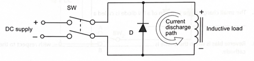
Freewheeling diodes
Used in many inductive loads and act as arc suppressors.
Zener diode
Behaves like a conventional diode in forward bias. Designed to run in reverse bias, blocks until critical breakdown voltage is reached, beyond this value it conducts. Maintains a constant voltage and used as a voltage regulator.
Zener voltage rating
The regulated voltage with rated reverse current flowing. Normal ratings are from about 2 V to 200 V in approximately 10% steps.
Wattage rating
Zener diodes are rated in terms of power (wattage) rather than current. Typical ratings are from about 250 mW to 50 W.
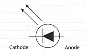
Light-emitting diodes (LEDs)
Gives off visible light when conducting. Specifically constructed with gallium arsenide, energy loss is primarily in the form of light. Have a low PIV rating of about 6V, should not be run in reverse bias.
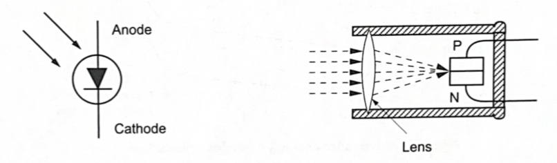
Photodiodes
Special PN junction diode in which light striking the junction increases the conductivity of the diode. Constructed with an opening in the case to focus light into the PN junction. Operated in reverse bias.
Bipolar-junction transistor
Can be visualized as a semiconductor sandwich. Back to back diodes.
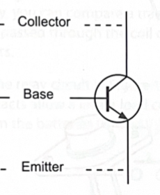
NPN Transistor
PNP Transistor
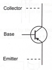
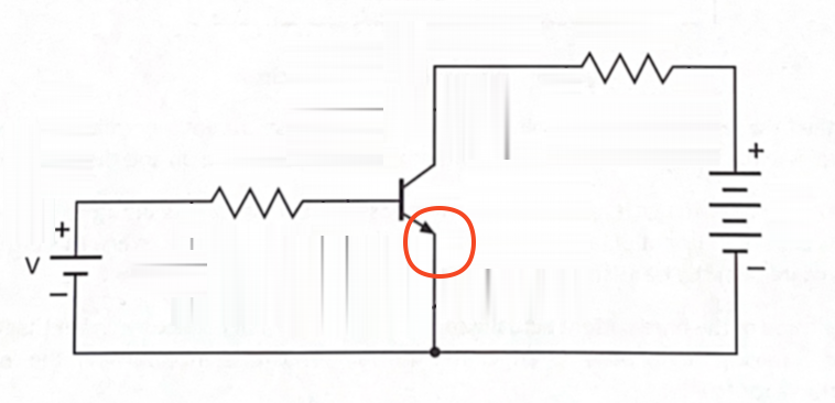
Transistor leads
Emitter, base, and connector.
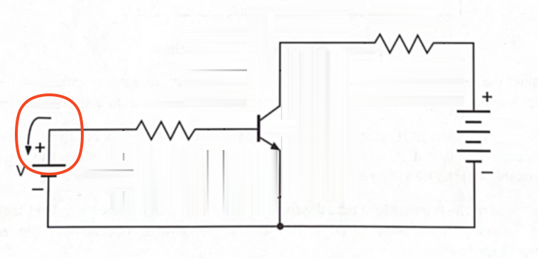
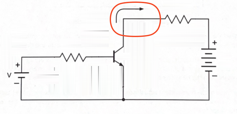
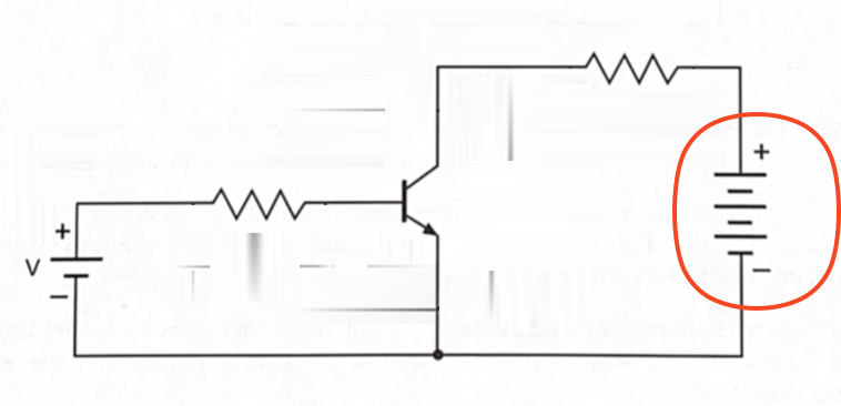
Control Circuit
Beta
\beta =\frac{I_{c}}{I_{b}}
Defines the transistors current gain or amplification factor. Usually a value of 100.
Amplifier
A device that controls a large current with a very small current.
Current relationship
Ie = Ib + Ic
Alpha
\alpha = \frac{I_{c}}{I_{e}}
Expresses current gain. Since the emitter current is always greater than the collector current, alpha is always less than 1.
Cut off
If base current is reduced to a value close to zero, then no collector current is allowed to flow.
Saturation
If the base current is increased to a value where the internal collector-to-emitter resistance is close to zero, then the maximum collector current (load) that flows is governed by Ohm’s law. Increasing the base current any further cannon allow any more collector current to flow.
Q
A transistor
Ib
Base current
Ic
Collector current
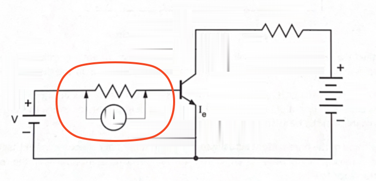
Ie
Emitter Current
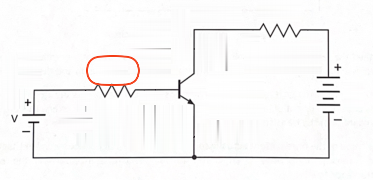
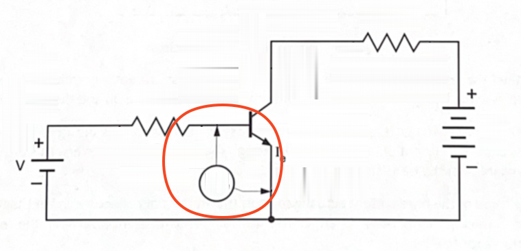
Rb
Base current resistance (control)
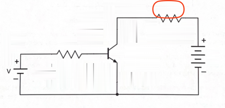
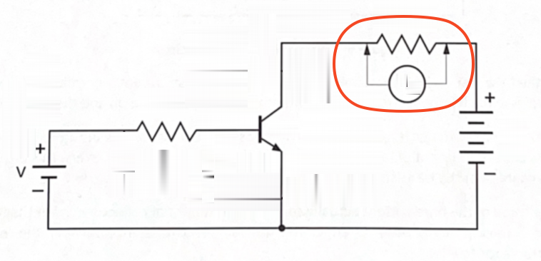
Rc
Collector circuit resistance (load)
VRb
Voltage drop across base circuit resistance
VRc
Voltage drop across collector circuit resistance
Vbe
Voltage drop across base-emitter leads
Vce
Voltage drop across collector-emitter leads
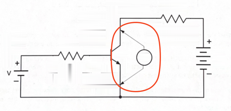
Vcb
Voltage drop across collector-base leads
Vcc
Voltage potential of the supply or source
Pentavalent elements
Arsenic, antimony, and phosphorus
5 valence electrons
Trivalent
Aluminum, boron, gallium
3 valence electrons