Chapter 3: Crystal Structure and Crystallography
1/30
There's no tags or description
Looks like no tags are added yet.
Name | Mastery | Learn | Test | Matching | Spaced | Call with Kai |
|---|
No analytics yet
Send a link to your students to track their progress
31 Terms
Short Range v. Long Range Order
No order: Monoatomic gases
Short range order (SRO): mostly liquids
Long range order (LRO): metals and alloys
If a crystalline material consists of only one large crystal, we refer to it as a single crystal
Crystal Structure
Solid materials may be classified according to the regularity with which atoms or ions are arranged wrt one another
A crystalline material is one in which the atoms are situated in a repeating or periodic array over large atomic distances; that is, long-range order exists such that upon solidification, the atoms will position themselves in a repetitive 3D pattern, in which each atom is bonded to its nearest-neighbour atoms
Some of the properties of crystalline solids depend on the crystal structure of the material, the manner in which atoms, ions, or molecules are spatially arranged
The atomic order in crystalline solids indicates that small groups of atoms form a repetitive pattern. Thus, in describing crystal structures, it is often convenient to subdivide the structure into small repeat entities called unit cells.
Thus, the unit cell is the basic structural unit or building block of the crystal structure and defines the crystal structure by virtue of its geometry and the atom positions within
Unit Cells
In describing crystal structures, it is often convenient to subdivide the structure into small repeat entities called unit cells.
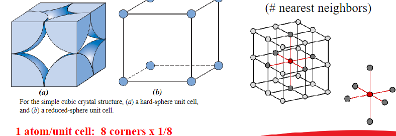
Simple Cubic Structure (SC)
Rare due to low packing density (only Polonium has this structure)
Close packed directions are cube edges
Coordination number = 6
APF: 0.52
R = 0.5a
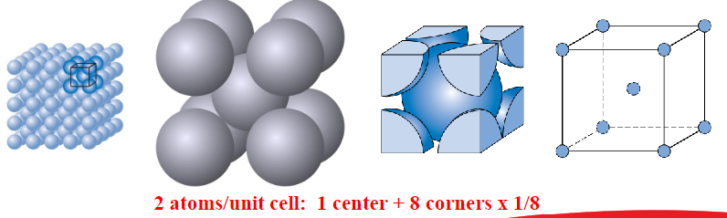
Body Centred Cubic (BCC)
Atoms touch each other along cube diagonals
Eg: Cr, W, Fe, Tantalum, Molybdenum
Coordination number = 8
APF: 0.68
4R = (sqrt3)a
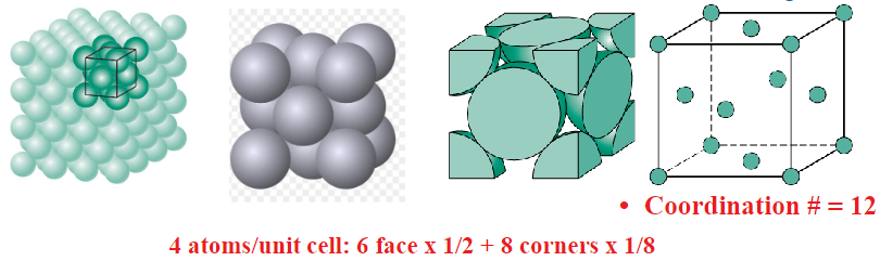
Face Centred Cubic (FCC)
Atoms touch each other along face diagonals
Eg: Al, Cu, Au, Pb, Ni, Pt, Ag
Coordination number = 12
APF: 0.74
4R = (sqrt2)a
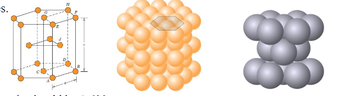
Hexagonal Closed-packed Structure (HCP)
The top and bottom faces of the unit cell consist of six atoms that form regular hexagons and surround a single atom in the centre
Another plane that provides three additional atoms to the unit cell is situated between the top and bottom planes
c/a ratio should be 1.633
Atomic Packing Factor
APF = Volume of atoms in unit cell/volume of unit cell
*assume hard spheres
APF = (atoms/unit cell)(4/3)(P)(R3)/a3
Stacking Sequence
FCC: ABCABC stacking sequence
HCP: ABAB stacking sequence
Theoretical Density, ρ
Density = ρ = (mass of atoms in unit cell)/(total volume of unit cell)
ρ = nA/VCNA
n = number of atoms/unit cell
A = atomic weight
VC = volume of unit cell = a3 for cubic
NA = Avogadro’s number = 6.022x10²³ atoms/mol
Single Crystal
For a crystalline solid, when the periodic and repeated arrangement of atoms is perfect or extends throughout the entirety of the specimen without interruption, the result is a single crystal
Single crystals exist in nature, but they may also be produced artificially. They are ordinarily difficult to grow, because the environment must be carefully controlled
Within the past few years, single crystals have become extremely important in many of our modern technologies, in particular electronic microcircuits, which employ single crystals of silicon and other semiconductors
Properties vary with direction (anisotropic)
Example: the modulus of elasticity in BCC iron
Polycrystals
Most engineering materials are polycrystals
Properties may or may not vary with direction
If grains are randomly oriented - will not vary with direction (isotropic)
If grains are textured - will vary with direction (anisotropic)
Anisotropic
Properties vary with direction.
Isotropic
Properties do not vary with direction.
Polymorphism
Two or more distinct crystal structures for the same material
Also called allotropy
Sometimes varies with temperature (titanium = HCP for low temp, and BCC for high, iron goes from BCC to FCC to BCC when increased to high temps)
Crystallographic Directions and Planes
Deformation under loading (slip) occurs on certain crystalline planes and in certain crystallographic directions. Before we can predict how materials fail, we need to know what modes of failure are more likely to occur
Other properties of materials (electrical conductivity, thermal conductivity, elastic modulus) can vary in a crystal with orientation
Lattice Directions, Planes, and Miller Indices
Miller indices used to express lattice planes and directions
x, y, z are the axes (on arbitrarily position origin)
a, b, c are lattice parameters (length of unit cell along a side)
h, k, l are the Miller indices for planes and directions - expressed as planes: (uvw) and direction: [uvw]
Family of direction is represented by <uvw>
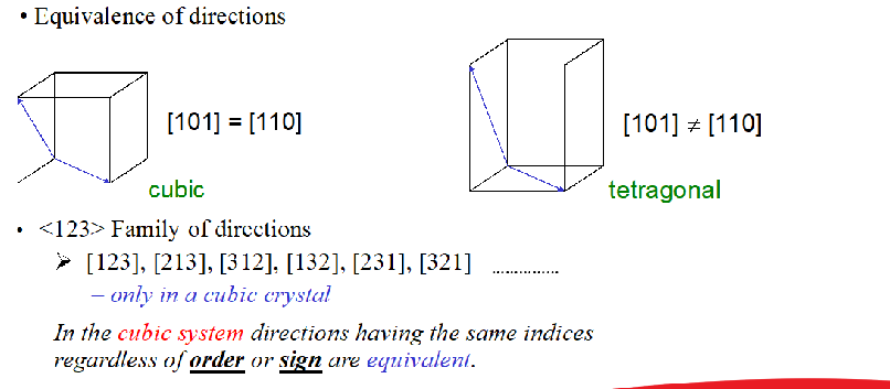
[100], [010], [001] are same family <100> cubic system
Convention for naming: NO COMMAS bw numbers
How to Define Direction
Crystallographic direction is represented by a vector connecting two points in the concerned direction
The vector is shifted so that one end falls at the origin
Vector projections on 3 axes are measured
They are revised to the smallest integer ratio
Now, the three indices measured is represented as [uvw], this is the direction
Miller Indices for Directions
Draw vector, define tail as origin
Determine length of the vector projection in unit cell dimensions, a, b, and c
Remove fractions by multiplying by the smallest possible factor
Enclose in square brackets
Families of Direction
HCP Crystallographic Directions
The three a1, a2, and a3 axes are all contained within a single plane (called the basal plane) and are at 120 to one another
The z axis is perpendicular to this basal plane. Directional indices, which are obtained as described earlier, will be denoted by four indices as [uvtw]
By convention, the first three indices pertain to projections along the respective a1, a2, and a3 axes in the basal plane
![<ul><li><p>The three a1, a2, and a3 axes are all contained within a single plane (called the basal plane) and are at 120 to one another</p></li><li><p>The z axis is perpendicular to this basal plane. Directional indices, which are obtained as described earlier, will be denoted by four indices as [uvtw]</p></li><li><p>By convention, the first three indices pertain to projections along the respective a1, a2, and a3 axes in the basal plane</p></li></ul><p></p>](https://knowt-user-attachments.s3.amazonaws.com/331239cc-901d-463b-bc22-4987d90b46ff.png)
Hexagonal Crystals - Miller-Bravais
4 parameter Miller-Bravais lattice coordinates are related to the direction indices as follows:
[u’v’w’] → [uvtw]
u = (1/3)(2u’ - v’)
v = (1/3)(2v’ - u’)
t = -(u + v)
w = w’
![<p>4 parameter Miller-Bravais lattice coordinates are related to the direction indices as follows:</p><p>[u’v’w’] → [uvtw]</p><p>u = (1/3)(2u’ - v’)</p><p>v = (1/3)(2v’ - u’)</p><p>t = -(u + v)</p><p>w = w’</p>](https://knowt-user-attachments.s3.amazonaws.com/93e5be5c-229e-4b6b-a60a-2df30ee0929c.png)
Miller Indices for Planes
Similar to directions, unit cell based 3 axis coordinate system is used for planes too
3 miller indices (hkl) used for cubic system and 4 indices (hkil) used for HCP system
Parallel planes are equivalent and has same miller indices
Family of planes represented by {hkl}
For a cubic system, if a plane and direction have the same set of miller indices, they are perpendicular to each other
Bracket Convention
Direction [uvw]
Direction Family <uvw>
Plane (hkl)
Plane Family {hkl}
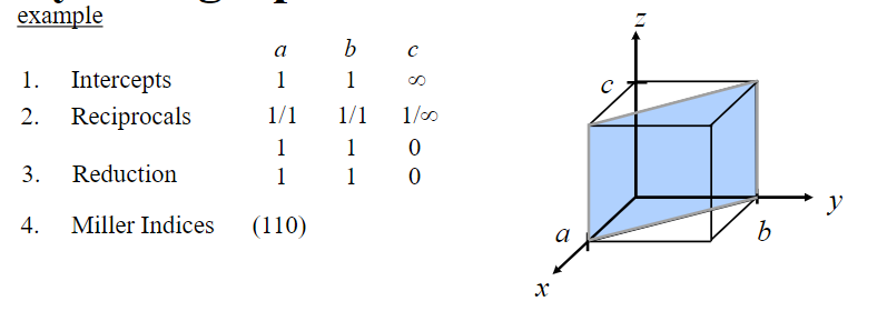
Miller Indices Procedure for Planes
Miller Indices: reciprocals of the three axial intercepts for a plane, cleared of fractions and common multiples. All parallel planes have the same Miller indices.
Algorithm
Read off intercepts of plane with axes in terms of a, b, c
Take reciprocals of intercepts
Reduce to smallest integer values
Enclose in parentheses, no commas
Slip Systems
Slip system is a combination of:
Plane (hkl) with highest PD
Direction [uvw] with highest LD lying in the plane
Linear and Planar Density
Properties in general, depend on linear and planar density
Examples:
Speed of sound along directions
Slip (deformation in metals) depends on linear and planar density
Slip occurs on planes that have the greatest density of atoms in direction with highest density
We would along closest packed directions on the closest packed planes
Atomic Densities
Linear Density:
number of atoms per length whose centres lie on the direction vector for a specific crystallographic direction
Linear Density = number of atoms centred on direction vector/length of direction vector
Planar Density:
Number of atoms per unit area that are centred on a particular crystallographic plane
Planar Density = number of atoms centred on a plane/area of the plane
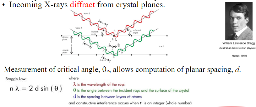
X-Ray Diffraction
Can be used to determine crystal structure
Identify unknown materials
Measure lattice parameters
X-rays are a form of electromagnetic radiation that have high energies and short wavelengths
Diffraction occurs whenever a wave encounters a series of regularly spaced obstacles that
Can scatter the wave
Have spacing comparable to the wavelength
X-ray wavelength (λ) ~ inter-atomic
Other techniques such as neutron or electron diffraction can also be used
Diffraction gratings must have spacings comparable to the wavelength of diffracted radiation
Can’t resolve spacing < λ
Spacing is the distance between parallel planes of atoms
Interplanar Spacing
Magnitude of the distance between two adjacent and parallel planes of atoms
It is a function of the Miller indices (hkl) as well as the lattice parameters
For example, for crystal structures that have cubic symmetry: dhkl=a/(sqrt(h2+k2+l2)) in which a is the lattice parameter (unit cell edge length)
X-Rays to Determine Crystal Structure