Electronic Principles, Semiconductor Materials (3a)
1/22
There's no tags or description
Looks like no tags are added yet.
Name | Mastery | Learn | Test | Matching | Spaced | Call with Kai |
|---|
No analytics yet
Send a link to your students to track their progress
23 Terms
What is the atomic structure of matter?
Matter is made of elements, each composed of atoms of the same kind.
Atoms:
Nucleus (protons + neutrons, except H) → dense, positively charged core
Electrons orbit nucleus at large distances relative to its size
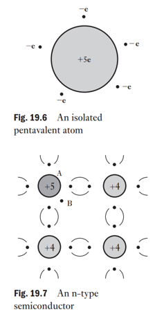
Electron: mass = 9.11×10−319.11 \times 10^{-31}9.11×10⁻³¹ kg, charge = −1.602×10⁻¹⁹-1.602 \times 10^{-19}−1.602×10⁻¹⁹ C
Proton: mass = 1.673×10−271.673 \times 10^{-27}1.673×10⁻²⁷ kg (1836 × electron), charge = +1.602×10⁻¹⁹+1.602 \times 10^{-19}+1.602×10⁻¹⁹ C
Neutron: no charge, mass ≈ proton’s mass
What are the atomic structures of hydrogen, helium, and carbon?
Hydrogen: 1 proton in nucleus, 1 electron orbiting (~10−1010^{-10}10−10 m orbit diameter).
Helium: Nucleus = 2 protons + 2 neutrons; 2 electrons in K-shell.
Carbon: Nucleus = 6 protons + 6 neutrons (charge = +6e); 6 electrons (2 in K-shell, 4 in L-shell).
What are conduction electrons and ions in atomic structure?
Electrons farther from the nucleus are easier to detach.
In metals, outer electrons can become free (conduction electrons), moving randomly but drifting under external influence.
An ion is an atom that has lost or gained electrons:
Lost electrons → Positive ion (more protons than electrons).
Gained electrons → Negative ion.
What is a covalent bond in atomic structure?
In a covalent bond, atoms share valence electrons with adjacent atoms.
Example: Atom A shares its 4 valence electrons with atoms B, C, D, and E.
Each shared pair of electrons orbits around both bonded atoms, holding them together.
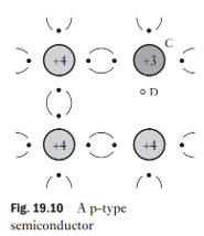
What is an N-type semiconductor and how is it formed?
by doping silicon/germanium with a pentavalent element (e.g., phosphorus, arsenic, antimony).
4 of the 5 valence electrons form covalent bonds; the 5th becomes a free electron.
Donor atoms (pentavalent impurities) introduce these free electrons.
The crystal remains electrically neutral, but conductivity increases due to mobile electrons.
Called (negative-type) semiconductor because electrons are the majority carriers.
How do donor atoms and an applied potential difference affect electron movement in an N-type semiconductor?
Donors provide fixed positive ions and equal numbers of free electrons.
More impurity → more free electrons per unit volume → higher conductivity.
With no potential difference (p.d.), electrons move randomly (no net drift).
With a cell connected (S positive, T negative), the electric field causes a drift of electrons toward the positive electrode (S), superimposed on their random motion.
Electrons leaving the semiconductor at S are replaced by electrons entering at T, keeping density
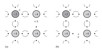
What is a P-type semiconductor and how is it formed?
Made by doping silicon with a trivalent element (e.g., indium, gallium, boron, aluminum).
Trivalent atom provides 3 valence electrons, leaving one incomplete bond (hole).
A hole is a vacancy that behaves like a positive charge carrier.
Holes attract electrons from neighboring atoms, causing the hole to move through the lattice.
holes are the majority carriers.
How do holes behave in a P-type semiconductor without an external electric field?
Holes move randomly between covalent bonds, at about half the speed of free electrons.
Random movement keeps hole density uniform, preventing charge buildup.
Each atom with a hole has a net positive charge (e).
The movement of holes can be regarded as the movement of positive charges within the P-type semiconductor.
What defines a P-type semiconductor and what are acceptors?
Holes move randomly, about half the speed of electrons, keeping hole density uniform.
Each atom with a hole is an ion with net positive charge (e).
Hole movement is treated as positive charge movement.
semiconductors are formed when silicon/germanium is doped with trivalent impurities.
These impurities are called acceptors because they can accept electrons from nearby atoms.
What happens at the junction of a P-type and N-type semiconductor in a diode?
P-type: has mobile holes + fixed negative ions (neutral overall).
N-type: has mobile electrons + fixed positive ions (neutral overall).
Diffusion: Holes move into N-region, electrons move into P-region.
This creates region A (negative) and region B (positive) near the junction.
These charges form a potential barrier at the junction, preventing further carrier migration.
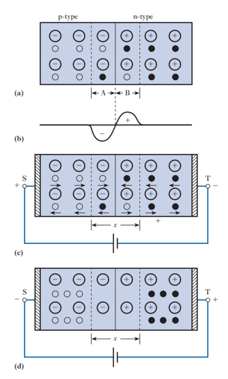
How does a diode behave under forward bias?
Forward bias: Positive voltage on P-side (S), negative on N-side (T).
Holes drift toward the junction in the P-region; electrons drift toward the junction in the N-region.
At the junction, electrons and holes combine, allowing current to flow.
Current results from:
Hole flow in P-region
Electron flow in N-region
Recombination near the junction
How does a diode behave under reverse bias, and what are minority carriers?
Reverse bias: P-side connected to negative, N-side to positive.
Holes move toward negative electrode, electrons toward positive, creating a depletion layer with almost no carriers → junction acts as an insulator.
Small current exists due to thermally generated electron–hole pairs.
Lifetime: ~50 ms in silicon, ~100 ms in germanium
Rate increases with temperature, reducing intrinsic resistance.
Minority carriers: Thermally generated carriers that are few compared to majority carriers.
P-type: holes = majority, electrons = minority
N-type: electrons = majority, holes = minority
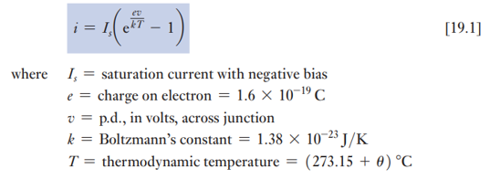
What is the reverse current in a silicon diode under reverse bias?
Reverse bias: Current remains nearly constant from ~0.1 V up to the breakdown voltage.
This constant current is called the saturation current (IsI_sIs).
In practice, reverse current slightly increases with voltage due to surface leakage.
What happens when one half of a crystal is doped with p-type impurity and the other with n-type impurity?
The p-type region has mobile holes and an equal number of fixed negative ions, making it electrically neutral.
The n-type region has mobile electrons and an equal number of fixed positive ions, also electrically neutral.
Thus, both regions are initially neutral before contact.
Why is the n-type semiconductor initially neutral?
Because it contains mobile electrons and an equal number of fixed positive ions, so the total negative charge of the electrons is balanced by the total positive charge of the ions — making the region electrically neutral.
What causes diffusion and drift of charge carriers in a semiconductor?
Diffusion occurs when there is a difference in carrier concentration between adjacent regions of a crystal.
Drift occurs only when there is a difference in electric potential (voltage) between two regions.
What happens when free electrons diffuse from the n-type to the p-type semiconductor?
As electrons diffuse into the p-type region, region A (near the junction on the n-type side) gains an excess negative charge, which repels further electron migration from the n-type to the p-type semiconductor.
What is the direction of the electric field in a p-n junction and what happens in the junction region?
in the semiconductor causes holes to drift right in the p-type region and electrons to drift left in the n-type region.
At the junction, free electrons and holes recombine, with electrons filling the holes (vacancies).
What happens when region B acquires a surplus of positive charge in a p-n junction?
becomes positively charged, preventing further migration of holes across the boundary.
These positive and negative charges accumulate near the junction, forming a potential barrier between the p-type and n-type regions.
What happens to charge carriers and recombination in a p-n junction?
The electric field causes holes to drift right in the p-type region and electrons to drift left in the n-type region.
At the junction, free electrons recombine with holes, filling their vacancies.
What causes current flow in a diode under forward bias?
An electron enters the n-region from the negative terminal and moves toward the junction.
Current in the diode results from hole flow in the p-region, electron flow in the n-region, and a combination of both near the junction.
What happens when the polarity of the applied voltage across a diode is reversed?
Holes are attracted to the negative electrode, and electrons to the positive electrode, creating a depletion layer (region x) with no free charge carriers except a few generated by thermal agitation.
What are minority carriers in a semiconductor, and how do they differ from majority carriers?
Minority carriers are thermally generated electrons or holes present in very small numbers compared to majority carriers.
In a p-type semiconductor:
Majority carriers: holes
Minority carriers: electrons
In an n-type semiconductor:
Majority carriers: electrons
Minority carriers: holes