application potential
 Call Kai
 Learn
Learn Practice Test
 Spaced Repetition
 Match
Match Flashcards
 Knowt Play
1/13

There's no tags or description
Looks like no tags are added yet.
Name | Mastery | Learn | Test | Matching | Spaced | Call with Kai | Chat |
|---|
No analytics yet
Send a link to your students to track their progress
14 Terms
Application potential
enhance efficiency of solar energy-based systems
photocatalytic hydrogen evolultion
reduce cost of NIR and SWIR imaging
access to advanced healthcare diagnostics making them wildely accessible giving societal impact
NIR sensing for food or medicine qualtiy control
NIR quality control works because different chemical bonds absorb NIR light at characteristic wavelengths, especially overtones and combination bands of O–H, C–H and N–H bend vibrations in the fingerprint region
By measuring how much NIR light is reflected or transmitted at selected wavelengths, we can infer properties such as moisture, fat content, ripeness or pharmaceutical composition.
how is this project linked to these SDGs?It contributes to sustainable development goals (SDGs) 3-7-11
SDG 3 - good health and well-being
biomedical imaging and sensing, low cost UC can make it more accessible
SDG7 - affordable and clean energy
can make larger fraction of solar spectrum usable
solar-driven photocatalysis for solar fuel production
SDG 11 - Sustainable cities and communities
make NIR camera’s cheaper for monitoring buildings, infrastructure, food quality
moisture ingress, insulation problems, or material degradation
how was this realized and how much time did it take? OLEDs present a key example of how organic materials research can lead to (huge) commercial success.[2] The global OLED market surpassed 47.2 billion USD in 2022 and is projected to grow at an annual rate of 14.4% from 2025 to 2032.[3]
“OLEDs are a good example of how fundamental organic-materials research can eventually create a major technology.
The first practical OLED was demonstrated in 1987,
the first commercial products appeared roughly ten years later,
OLED TVs about twenty years later.
Commercial success required decades of improvements not only in emitters, but also in charge-transport layers, lifetime, encapsulation, pixel electronics and scalable manufacturing. That shows that translating a new organic optoelectronic concept into a mature technology is a long process, but one with potentially very large impact.
What is TRL?
Even though the individual impact of a single Ph.D. student on bringing UC technology to the market might be limited, we have a clear strategic vision on how to translate our findings to applications for specific users (and also valorize them in higher-TRL follow-up projects), strongly facilitated by the integrated team efforts at IUMAT.
TRL stands for Technology Readiness Level. It indicates how mature a technology is, from
basic research at TRL 1
to a commercial product at TRL 9.
My PhD mainly focuses on the lower TRLs by improving the materials and proving device concepts, while follow-up projects can move the technology toward prototypes and real-world applications
green?
definition of STH?
UCQE of 10-20% realistic?
what is the flemish hydrogen strategy?
* Incorporation into a photocatalytic system. Up-conversion has clear benefits in photocatalysis. The most promising candidates for green solar hydrogen production are wide-bandgap photocatalysts such as TiO2, with an absorption limited to the UV and short-wave VIS. The solar-to-hydrogen conversion efficiency (STH) is, however, limited < 5% when relying solely on UV light. By extending light absorption to include the VIS and NIR, the STH increases significantly. To achieve a 10% STH, an UC device that converts VIS/NIR to UV photons would need an UCQE of about 10–20%.[4]. To effectively minimize the overhead associated with integrating innovative UCs into photocatalytic systems, it is essential to use low-cost materials, which are currently not available but are key to making this technology both feasible and economically viable. The NIR absorbers envisaged in my Ph.D. directly address this challenge. The project also aligns nicely to the Flemish Hydrogen Strategy.[5]
What does “green hydrogen” mean?
Green hydrogen is hydrogen produced without fossil-fuel CO₂ emissions, using renewable energy.
STH = solar-to-hydrogen efficiency: the fraction of incident solar energy that ends up stored as chemical energy in hydrogen.
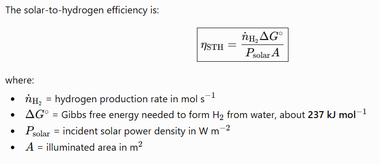
Around 10% is often cited as a target for economically attractive photocatalytic water splitting
Is an UCQE of 10–20% realistic?
As shown in Figure 1b, taking the photocatalytic H2 evolution reaction as an example, the solar-to-hydrogen conversion efficiency (STH) would be limited to below 5% when relying solely on UV light up to 400 nm, even if the photocatalytic quantum efficiency (QE) reaches 100%.[7] However, by extending the light absorption range to include the visible and NIR regions up to 700 and 1000 nm, respectively, the maximum STH can significantly increase to 25% and 47%.[8] For achieving a target STH of 10%, a photocatalyst with an absorption threshold of 1000 nm would only require a QE of ≈22%.
22% of incident photons lead to reaction
5% is already UV, so would need an additional 15% of UV light, this can come from UC of visible and NIR light
Your self-powered diode UC currently reaches about 1.9% EUE, so 10–20% would require substantial improvements in OPD EQE, photon absorption/current matching, OLED efficiency, outcoupling, and probably a lower-turn-on-voltage emitter. For UV upconversion, it may be even harder because a UV LED requires more voltage, potentially requiring more OPDs.
For photocatalysis we are not restricted to using the same NIR detecting OPDs because spatial information does not need to be preserved. we could therefore develop a tandem broadband UC in wich different OPDs harves different parts of the visible and NIR spectrum. The same photons do not need to be split over each layer so a larger current can be generated. Also, higher bandgap OPDs can generate larger photovoltages, reducing the number of PDs so the ceiling UCQE could be increased. The only limitation would still be current matching, but a higher UCQE would certainly be more achievable.
Vlaanderen launched its hydrogen strategy in 2020 with the ambition of becoming a European leader in hydrogen technology and building a strong Flemish hydrogen ecosystem. Its fi
photocatalytic QE = useful electrons or porduct molecules / photons
UCQY vs UCQE vs EUE
UCQY and UCQE are used interchangably in the proposal where a distincition is made between internal and external
UC efficiency = number of upconverted pphotons / number of incoming low-energy photons
This photon-to-photon conversion yield (UCQY) was measured for photons outcoupled to air. The outcoupling factor from organics on glass substrates with an effective refractive index of 1.4-1.5 is approximately 0.25, which means that the effective internal UCQY is on the order of 4%
in the paper they refer to the EUE = external upconversion efficiency which is the same as the external UCQE
We will start by investigating the photo-degradation of Rhodamine B in the presence of TiO2 nanoparticles under UV, VIS, and NIR light of various intensities. The UC will be encapsulated between glass slides and submersed in the photocatalytic dispersions.
how is this useful?
It is useful as a simple proof-of-concept experiment to show whether the UC can actually drive a photocatalytic reaction, rather than only showing that it emits light.
TiO₂ normally needs UV photons to generate electron–hole pairs. Those charges can form reactive species such as OH∙ and O2-.(superoxide), which degrade Rhodamine B. By following the decrease in Rhodamine B absorption with UV–vis spectroscopy, you get an easy quantitative measure of photocatalytic activity.
Testing UV, VIS and NIR at different intensities lets you establish three things:
UV: gives the baseline activity of TiO₂ when it is excited directly.
VIS/NIR without UC: shows how little activity TiO₂ has when the photons are below its bandgap.
VIS/NIR with UC: shows whether the UC converts those low-energy photons into photons energetic enough to activate TiO₂.
Rhodamine B (xanthene dye) is mainly used as a convenient model compound because it is water-soluble and has a strong, easily measurable absorption band
In a second demonstration, we will bring a reflective UC in optical contact with a high bandgap photocatalytic electrode and determine its performance increase. Within the H2-lab at IUMAT, we have a LED based light-source simulator available which can generate monochromatic and solar spectra at various intensities. A first stack recipe which can readily be used to implement in a photocatalytic system incorporates a blue/UV emitter (e.g., commercially available Cz-PS and Cz-MPS[6]) in the reference stack.
how does this work?
what is optical contact?
what is Cz-Ps and Cz-MPS, what are their structures?
What does “optical contact” mean?
It means that the UC and photocatalytic electrode are placed directly against each other, or separated by only a very thin optically transparent interface, rather than having a large air gap between them.
The process is:
UV photons are already absorbed directly by TiO₂ and drive photocatalysis.
Much of the visible/NIR light passes through because its photon energy is below the TiO₂ bandgap.
The OPDs in the UC absorb those transmitted VIS/NIR photons and generate photocurrent and photovoltage.
This electrical energy drives a blue/UV OLED.
The OLED emits higher-energy photons back toward TiO₂.
TiO₂ absorbs these photons, creates electron–hole pairs, and these charges can drive reactions such as water splitting.

Cz-PS and Cz-MPS (diphenylsulfone (PS))
= carbazole-based TADF (thermally activated delayed fluorescence) emitters that can be used for blue/UV OLEDs
When electrons and holes recombine in an OLED, statistically you form roughly:
25% singlet excitons
75% triplet excitons
Singlets emit efficiently, but triplets decay mostly non-radiatively because relaxation to groundstate is spinforbidden. A TADF molecule is designed so the energy difference between the triplet and singlet is very small, so at room tempertaure reverse intersystem crossing (RISC) can generate S1 which can emit as fluorescence. This means 75% triplets are recovered
Ir-based phosphorescent emitter: the heavy Ir atom gives strong spin–orbit coupling, which makes intersystem crossing efficient and also allows the normally spin-forbidden triplet transition:
T1→S0+hν
So both singlet and triplet excitons are funneled into triplet states and emit by phosphorescence. This is why Ir-based OLEDs can approach ~100% internal quantum efficiency.
TADF doesn’t emit via phosphorescence because no heavy atom, so spin-orbit coupling is much weaker
2nd demonstrator to showcase the potential of next-generation up-conversion technology
* Incorporation into a NIR-imaging system. UCs have exciting applications in NIR imaging, enabling in vivo and deep tissue imaging of the human body. However, these UCs require a high UCQY of at least 5%, with illumination intensities < 10 mW/cm² to be used in such applications. These requirements have not yet been met. The diode-based approach allows self-powered (i.e., without any external voltage) photon up-conversion that scales linearly with incoming light intensities, thereby maintaining a high UCQY at low intensities (efficiency remains the same but output becomes lower while for non-linear the efficiency drops), enabling devices to be used in low-cost, high-quality NIR imaging with a simple smartphone camera in the range of 700 to 1000 nm.[8]
so the UC allows pixelless imaging because of the limited latheral movement of the charge carriers, but the LED, doesn't it emit in all possilbe direction and lose this spatial informaiton?
The important thing is that the photon is generated at the correct position in the OLED.
suppose the NIR light hits position x1
creates photocurrent at x1,
and OLED emission at x1
the photon is emitted in many directions but they all originated from the same point
The imaging lens collects a range of these rays and focusses them onto the corresponding point on the Si camera sensor
photons from x1 on UC are focussed via lens on x’1 on camera
this is also how normal imaging works: objects scattor or emit light in many directions, and a lens recontructs the spatial image because it maps light according to where it originated from.
Imaging demonstration of organic UC
First demonstration: UC infront of a normal camera
object is illuminated with NIR light, NIR is absorbed/transimitted
the NIR imag is projected onto the UC with lensens
the lense preserve spatial information
bright parts of the NIR image illuminate the corresponding positions on the UC more strongly
the UC converts NIR into visible light while preserving the spatial information
a second lens project the visible image onto a normal Si camera (lowcost rasberry pi camera) 25-75 euros
the UC itself is pixelless, the camera provides the acutal pixels and readoutelectronics
it was shown to have a feature size of 50 µm = smallest detail the imaging system can distinguish, so eg. if two lines are 50 µm apart they are visualized separatly if closer, they blurr together
Second domonstrion: will be to place the UC film directly onto the light-sensitve camera element
the UC is placed directly on top of the silicon image sensor
NIR image is locally converted into visible light directly aboe the corresponding CMOS pixels
so no separate lenses are needed
The main challenges
is that when the UC is directly on the sensor, you have to make sure the emitted visible light does not spread too far sideways before entering the Si pixels
the optical stack would have to be optimized so that NIR enters from the outer side while the upconverted visible light is preferentially emitted toward the Si sensor
Stakeholeders to invite to our workshop
Survey
we don’t have a complet overview yet of potential users, companies,…
during the project we could therefore organise a workshop to bring stakeholders together
this way we can identify who could benefit from it, what performance they would require and whether there is commercial interest
Previous stakeholders UHasselt has worked with:
MIRIS = monolithic infrared image sensor
SBO project running fro 2016-2019
goals= make low-cost NIR image sensor by depositing thin film organic photodetector directly onto a silicon CMOS readout chip
this project already connected UHasselt with IR imaging stakeholders
FLOWS = flexible organic wearable sensors
new SBO project
developing a flexible organic-electronics platform for wearable monitoring and wound-healing applications
brings stakeholders in flexible substrates, wearable integration, encapsulation and biomedical users
RISE-UP = REDEFINING INFRARED LIGHT AS A USABLE RESOURCE THROUGH LOW-COST, SELF-POWERED UPCONVERSION
EIC pathfindinder application submitted by my promotors = funding program by EU to support research for high-risk, high-gain scientific breakthroughs
it will combine organics, perovskites and quantum dots to develop flexible, large-area NIR to visilbe foil with more than 25% internal UCQE at low light intensities
my contribution will be to develop improvid organic NIR aborbers and photodiodes
RISE-UP than adds engineering, modelling and partners such as COMATE to translate these materials into real applications
Belgian company stakeholders:
COMATE
belgian engineering company that turns technologies or prototypes into production ready hardware
they can help the transition from laboratory UC to an integrated prototype
they are part of RISE-UP and can also help in investigating which markets and companies in flanders and europe might actually buy or use this technology
Imaging
XENICS
design and manufacture of IR detectors and cameras, especially SWIR InGaAs sensors for medical imaging, security, process monitoring
part of exosens and spin-off of IMEC
they could tell us whether UC-based Si camera is thecnologically or commerically intersiting compared to InGaAs camera’s
FUJIFILM
develops medical imaging/endoscopy systems and materials of imag sensors, including IR selective materials for NIR sensing
Agfa
background in medial imaging and imaging technology
sensors and electronics
Melexis
Belgian semiconductor company focussed on senor IC’s including IR sensor arrays and thermal imaging sensors
NXP
semiconductor company making sensor and image processing electronics
flexible manufacturing
Quad industries
printed flexible electronics
UC towards flexible foils, wearable sensors
Materials and scale-up
Umicore
belgina advanced materials and recycling company with expertise in semiconductor materials and circularity
relevant for material supply, electrodes, sustainable sourcing
Solvay
supply high-purity marierials and process chemicals for electronics and semiconductor processing
International companies
Samsung and LG
end-users for display and smarphone imaging
FLUXIM AG
involved in RISE-UP
swiss company that develops simulation software and optelectronic measurement equipment
can help answer: which materials and layer thicknesses give the best UC performance
Valorization of the project
Valorization = turing results into economic or societal value (prototype, licensed technology, spin-off company) This can initially be publications and new knowledge, but promising results can later lead to collaborative projects, patents, industrial partnerships or potentially a spin-off.”
Different options towards valorization are considered: (valorization is not one project but the whole process, these programs are tools to fund different stages of that process)
By others
SBO = strategisch basis onderzoek
this PhD gives promising results but need further research then a larger team could apply to FWO for an SBO for a larger research project to solve remaining challenges
CONCEPT project (UHasselt)
we can apply for a CONCEPT project that will provide funding to investigate where the technology is most useful and who would want it
eg. via stakeholder workshops, market analysis
POC = proof of concept project (UHasselt)
apply for funding to develop and test a concret prototype
eg. put UC directly onto a CMOS camera and demonstrate that it works under realistic conditions
By me personally
VLAIO = Vlaams Agentschap Innoveren & Ondernemen (innovation mandate)
you apply as psot-doc to continue developing research toward economic use, either together with existing company or by creating a spin-off
To achieve even broader exposure we can host a webinar:
present the UC technology to a broader group of companies and potential users, which can help identify new partners, applications, and market interest.
Securing IP will be crucial:
= protect valuable inventions before they are published
IP = intelectual property
if I invent a new absorber or OPD, UHasselt could protect it as its own IP
if developed with other groups or partners (the UCs incorporating my material) this is owned together = joint IP
TTO = technology transfer offic - at UHasselt
they help research to move inventions toward practical use by assessing
patentable
novel
useful
non-obvious
who owns it - IP on a ship
how it could be licensed to a company
Invention disculure form
= first document you submit to TTO when you think you invented something valuable and should be patented
it contains
what you invented
what is new about it
who contributed
what data supports it
if already published
possilbe applications
Patents protect your invention from being commercially exploited by others.This can create a protected position for further development and can support licensing, industrial collaboration, or the creation of a spin-off.
FWO
fonds wetenschappelijk onderzoek - vlaanderen