Electronic Circuit Design 2 - Week 3 PSD asynchronous
1/24
There's no tags or description
Looks like no tags are added yet.
Name | Mastery | Learn | Test | Matching | Spaced |
|---|
No study sessions yet.
25 Terms
what does a PSD circuit do?
It is a circuit which recovers the phase and amplitude of a sin wave signal
what does PSD stand for?
Phase sensitive Demodulation
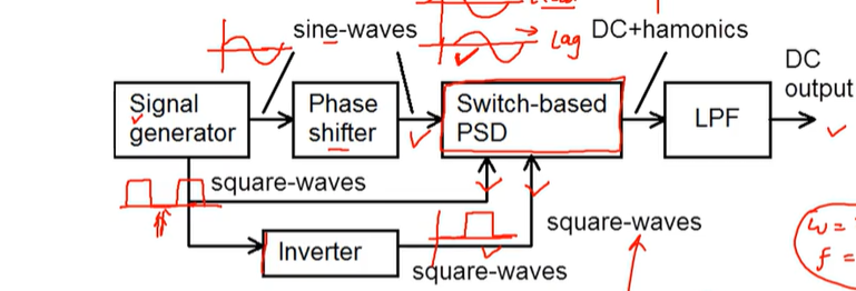
Draw the overall arrangement for the PSD Circuit including waveforms every time there is a change in the circuit.
note where it shows there is a lag waveform it could also be leading depending on circuit but screenshot could not capture it.
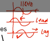
Draw a sinwave- which has gone through a switch based PSD circuit which causes it to become lagging and also leading. draw the original sin wave going through the origin with no phase shift.
leading can also be referred to as forward
lagging can also be referred to as backwards or delay circuit
what is the purpose of the LPF in the PSD circuit
it removes the high frequency harmonics of the signal
if the original sin waves signal is 1KHz what is the frequency of the resulting signal after going through the PSD circuit but before going through the LPF and why
2Khz as the resulting signal is effectively rectified but with phase it will always have a frequency of twice that of the original sin wave
what is an example of another demodulating method which is not PSD
a rectifier circuit
what is the difference between a rectifier circuit and a PSD circuit
the rectifier circuit is not sensitive to Phase whereas the PSD is even though both waveforms may look similar.
what is the PSD circuit commonly used for?
it is commonly used in signal conditioning circuits for data acquisition/ instrumentation.
what are the two popular types of PSD circuit?
Switch based PSD
PSD based on an analogue multiplier
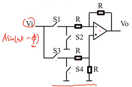
Draw the circuit for the switch part of the switch based PSD signal and also say what electronic components it consists of. include the label for the generic formula for Vi
it consists of an op-amp, 4 analogue switches and 4 resistors all of the same value.
what type of signal is used to control s1,s4 and s2,s3 for a switch based PSD circuit
2 complementary square wave signals are used
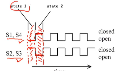
draw the signals used to control the switches s1,s2,s3,s4 for a switch based PSD, include states.
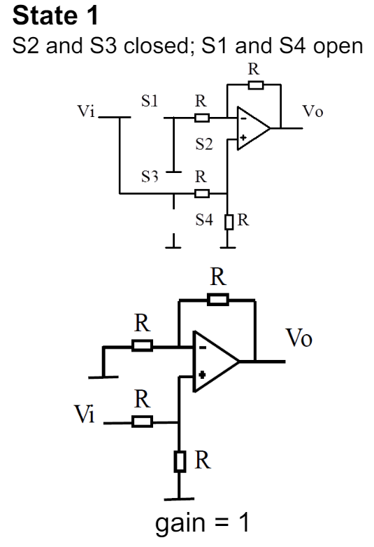
draw the circuit for the switch based PSD circuit in state 1 when the switches s2,s3 are closed.
draw two circuits the full circuit with all switches and then also the simplified circuit.
state the gain and also what type of circuit the simplified circuit is.
a non inverting amplifier
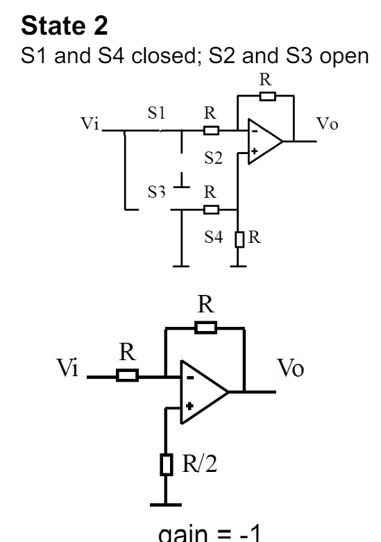
draw the circuit for the switch based PSD circuit in state 2 when the switches s1,s4 are closed.
draw two circuits the full circuit with all switches and then also the simplified circuit.
state the gain and also what type of circuit the simplified circuit is.
an inverting amplifier
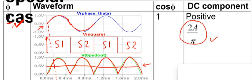
for the special case where the phase shift is 0 degrees draw the waveforms of the input signal, the square wave and then the resulting output signal. include the value of cos(theta) where theta is the phase shift and also the value of the DC component.
include states on square wave waveform and line indicating dc component on resulting output waveform
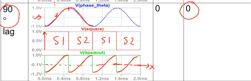
for the special case where the phase shift is 90 degrees lagging draw the waveforms of the input signal, the square wave and then the resulting output signal. include the value of cos(theta) where theta is the phase shift and also the value of the DC component.
include states on square wave waveform and line indicating dc component on resulting output waveform
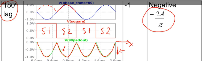
for the special case where the phase shift is 180 degrees lagging draw the waveforms of the input signal, the square wave and then the resulting output signal. include the value of cos(theta) where theta is the phase shift and also the value of the DC component.
include states on square wave waveform and line indicating dc component on resulting output waveform
note dc component line is not shown here in pic but it is a straight line through -0.5V
for the special case where the phase shift is 270 degrees lagging draw the waveforms of the input signal, the square wave and then the resulting output signal. include the value of cos(theta) where theta is the phase shift and also the value of the DC component.
include states on square wave waveform and line indicating dc component on resulting output waveform
do at a later date.
write down the mathematical derivation for finding the output of a PSD circuit.
note: a factor of 1/2pi is taken outside the integral as we are caluclting the average value of a sin wave over 1 period. 1/2pi is equalivent to 1/time period.
note: for the second last line all the terms inside sqaure brackets can be considered to be cos(theta) hence when added together you get 4cos(theta)/2 pi which then simplifies to the last line. I am not sure why they are all cos(theta)
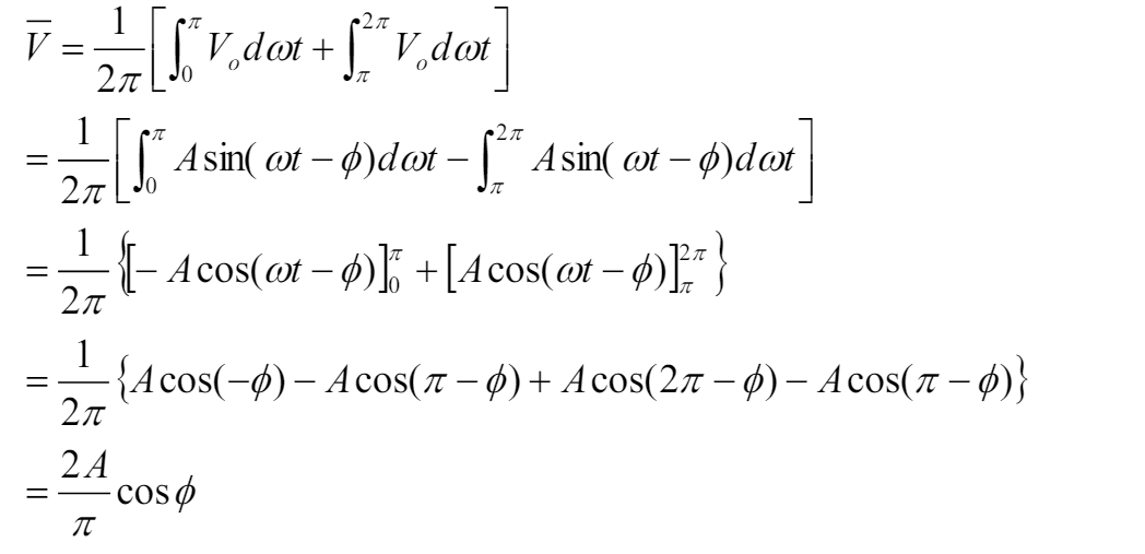
what is noticeable about the mathematical formula for the output of a psd circuit.
it has an A and a theta term meaning the output depends on the phase and the amplitude of the original signal.
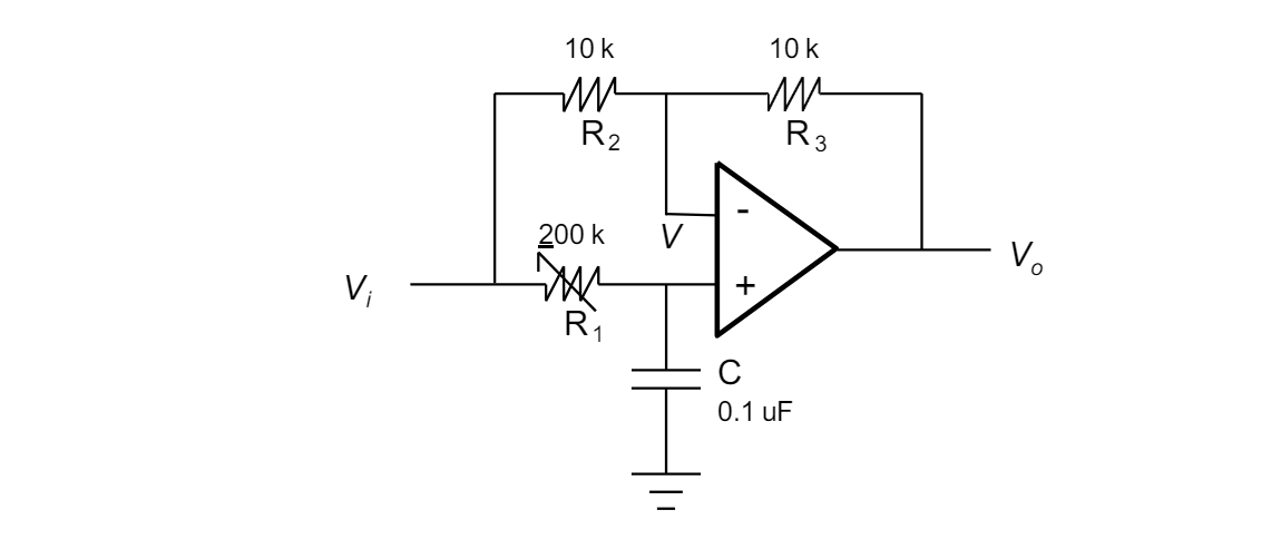
draw the phase shifter circuit
do the derivation to find the transfer function of the phase shifter circuit using circuit analysis.
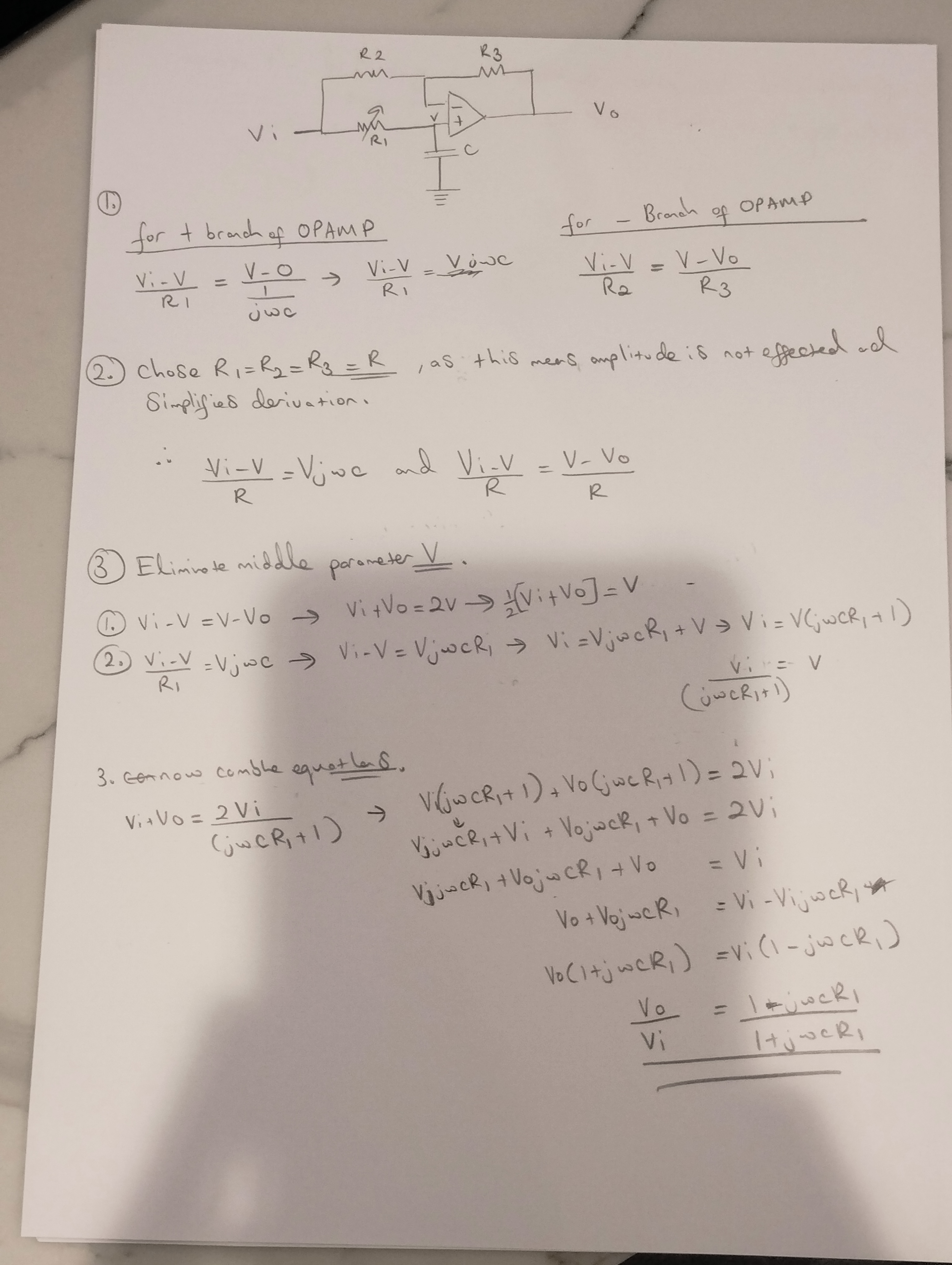
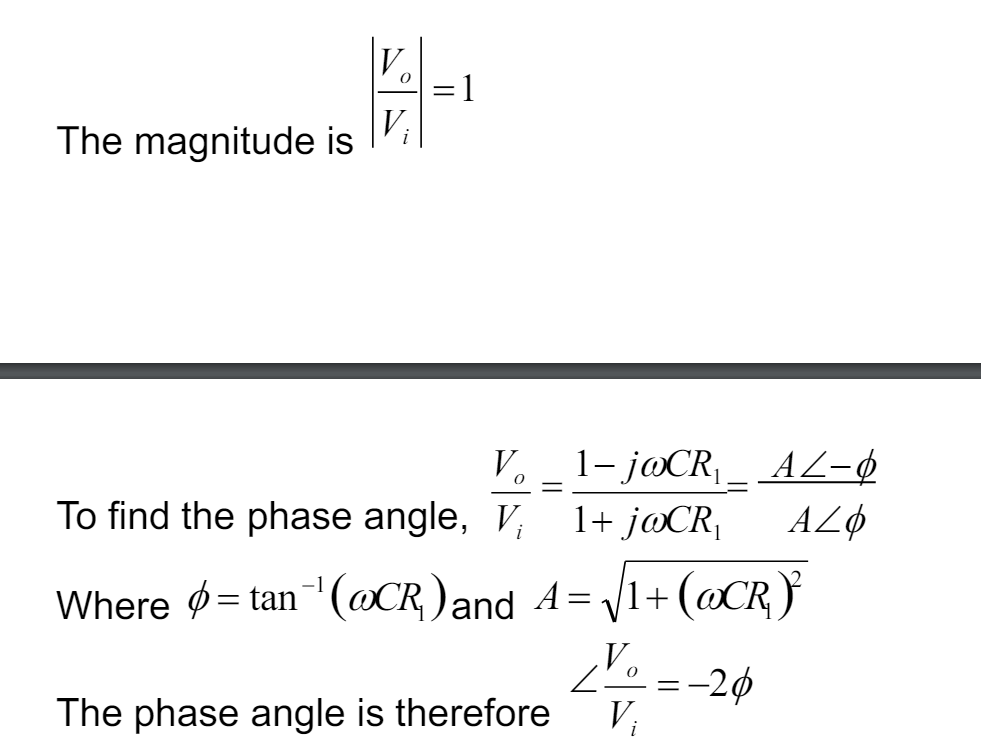
write the equations to calculate the phase angle and magnitude of the phase shifter circuit when all resistors are equal
note to in the picture it shows how to calculate theta and A by hand but you can just use a calculator to do this
for the phase shifter circuit what physical component do we use to adjust the phase angle of the output and how much can we adjust the phase angle by
we can use the variable resistor R1 and we can adjust the output between 0 and -180 degrees.