Nanotech for Sustainable Energy
1/68
There's no tags or description
Looks like no tags are added yet.
Name | Mastery | Learn | Test | Matching | Spaced | Call with Kai |
|---|
No analytics yet
Send a link to your students to track their progress
69 Terms
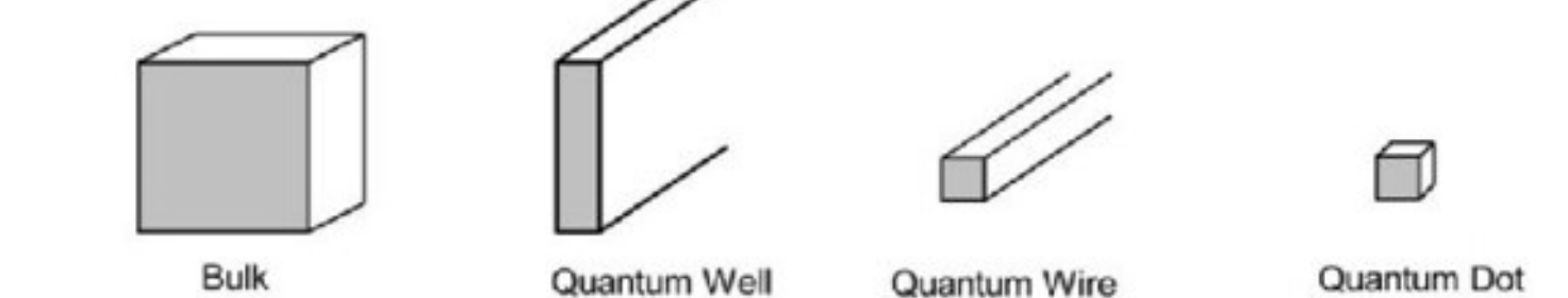
0D nanostructure
nanocrystals (e.g. quantum dots, which typically means a nanocrystal of semiconductor material);
often synthesized by ‘colloidal method’ using surfactant/ligands to control size, shape, and crystal facets, therefore controlling their physical/chemical properties.
1D nanostructure
nanowires or nanotubes (or related, such as fibers, rods);
common synthetic methods include vapor-liquid-solid (VLS) synthesis, electrospinning method, template-assisted deposition, chemical etching
2D nanostructure
nanosheets or nanoplates (such as graphene, MoS2 sheets, etc);
common synthetic methods include liquid exfoliation, mechanical cleavage, self-assembly, chemical vapor deposition (CVD).
3D nanostructure
in a more general term, once collective low-dimensional nanostructures assembled into 3D architecture,
such as photonic crystals or 3D nanowire/tube vertical arrays;
common methods include self-assembly, selective etching (especially to form vertical arrays), chemical/physical vapor deposition (CVD), etc.
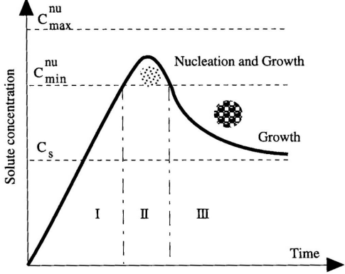
Approaches for size control of nanocrystals (2)
Separate nucleation and growth steps, as below: controlling nucleation time as short as possible to have more nucleus of uniform size for further growth.
Avoid aggregation during solution synthesis by introducing surfactants coatings or electrostatic repulsion between crystals.
Nucleation of nanocrystals
How can you control the shape of nanocrystals?
By understanding and manipulating the surface energy of different crystal facets.
selective binding, where surfactants bind to specific surfaces and alter the surface energy, leading to anisotropic growth and different shapes.
3 different carbon allotropes
Graphite, Diamond, CNT
Fullerene, Amorphous carbon
Sp3 Carbon
Diamond or Lonsdaleite
tetrahedral bonding
Diamond: transparent, insulator, very hard
Sp² Carbon
Trigonal planar bonding
graphene, amorphous carbon
Graphite: lubricant, semi-metal, opaque black
distorted Sp² Carbon
CNT * c60
Cnt: metallic/semiconducting, mechanically strong, high thermal conductivity
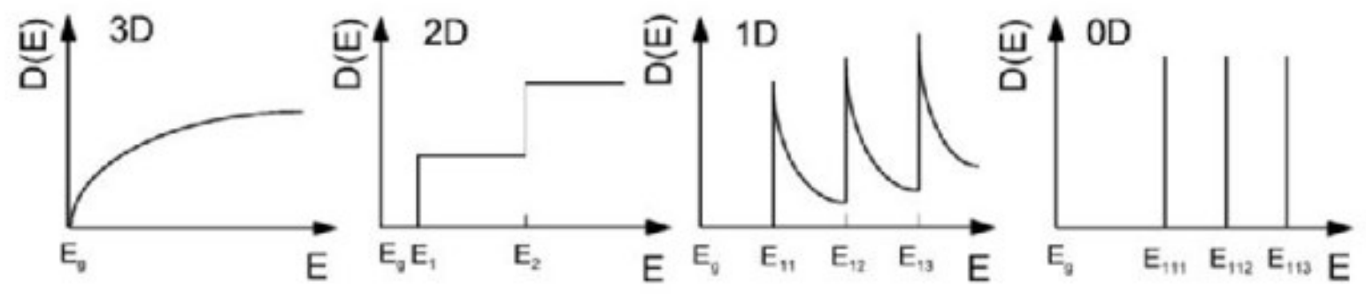
What is density of states?
the number of different states at a particular energy level that electrons are allowed to occupy
Working mechanism of solar cells
photon with large energy enters (larger than bandgap)
Electron hole pair generation
electron-hole separation through built-in voltage enabled by p-n junction
photo-induced current generated
Why is the p-n junction needed for solar cells?
The space charge regime generated by p-n junction below shows the band-bending to create built-in E-field to guide electron-hole to separate and move to two opposite contacts.
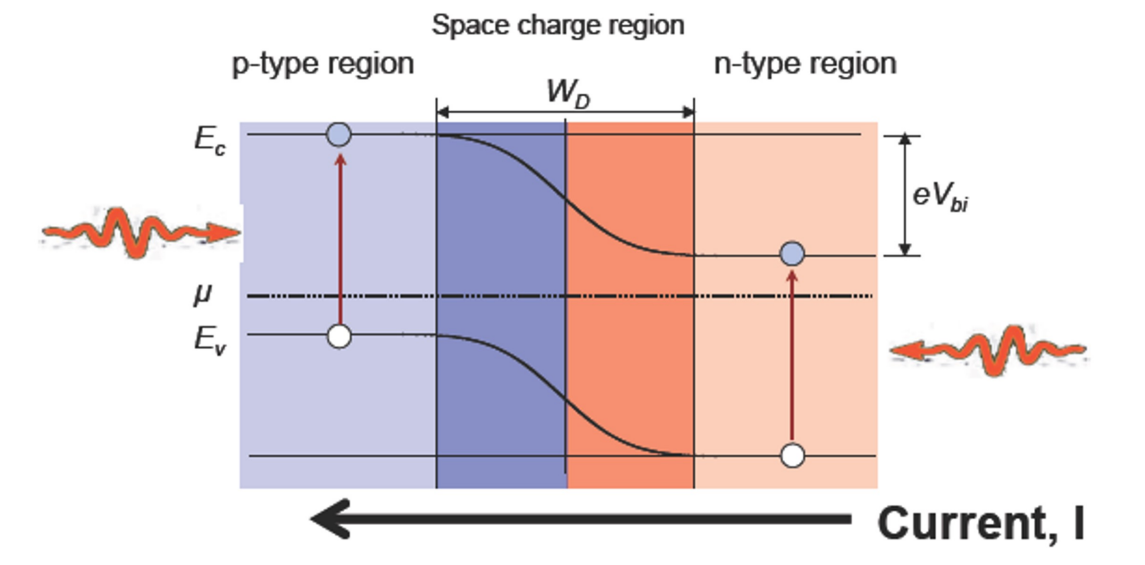
Why is the depletion region mainly in p - region? (when you connect highly doped N type to lightly doped p-type)
Since NA << ND (heavily doped n-type), it is an asymmetric junction and the total current is dominated by the most heavily-doped side of the junction, and
the space charge region width is dominated by the lightly-doped side of the junction (Xn << Xp); as clearly from
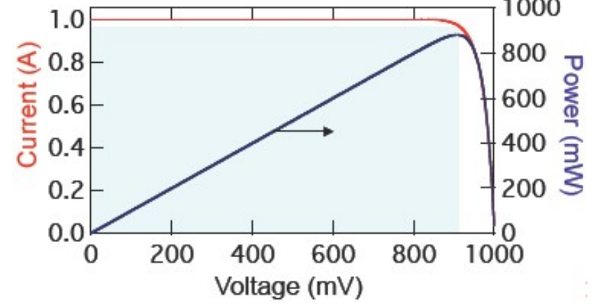
Please sketch a simple solar cell characteristic curve for ideal solar cell
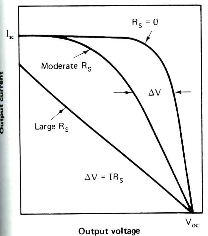
Limiting series resistance
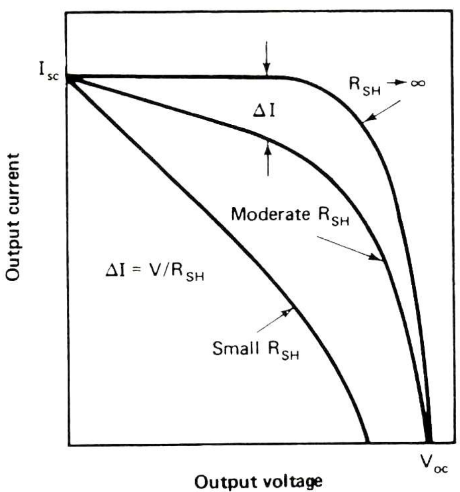
Limiting shunt resistance
Solar cell circuit
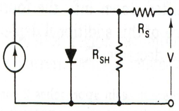
Explain parameters in solar cell (lecture 5)
MOCVD
deposition technique for depositing thin layers of atoms onto a semiconductor wafer
allows precisely controlled thickness, to create a material which has specific optical and electrical properties
by chemical reaction and not physical deposition
Typically it is not in vacuum, instead from precursor gas sources
MBE
Molecular Beam Epitaxy:
High or ultra high vacuum
slow process
but the absence of carrier gases as well as the ultra high vacuum environment result in the highest achievable purity of the grown films
Very expensive
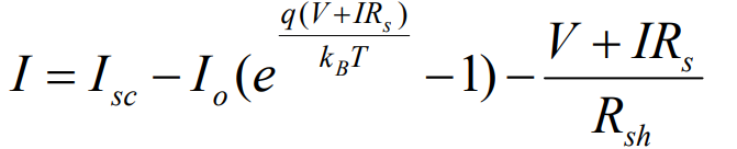
For multi-junction solar cells, please draw a schematic device structure of triple-junction solar cell based on GaInP, GaAs, Ge..
three p-n junctions made from GaInP, Ga(In)As and Ge stacked on top of each other
each layer with a band gap energy higher than the layer below it
and assembled with low resistive tunnel junctions..
In triple junction, Why is the order of placing different junction layer?
Photons with energy lower than the band gap pass to the lower junction, and photons with energy lower than this threshold traverse to the lowest junction in the stack
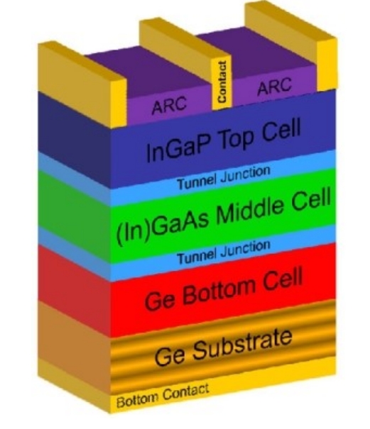
Schematic of CdSe-based solar cell
advantages of CdTe PV
smallest carbon footprint
lowest water use and shortest energy payback time of all solar technologies (both energy & environmental impact)
optimum bandgap ~ 1.5 eV for solar spectrum adsorption.
20% efficiency
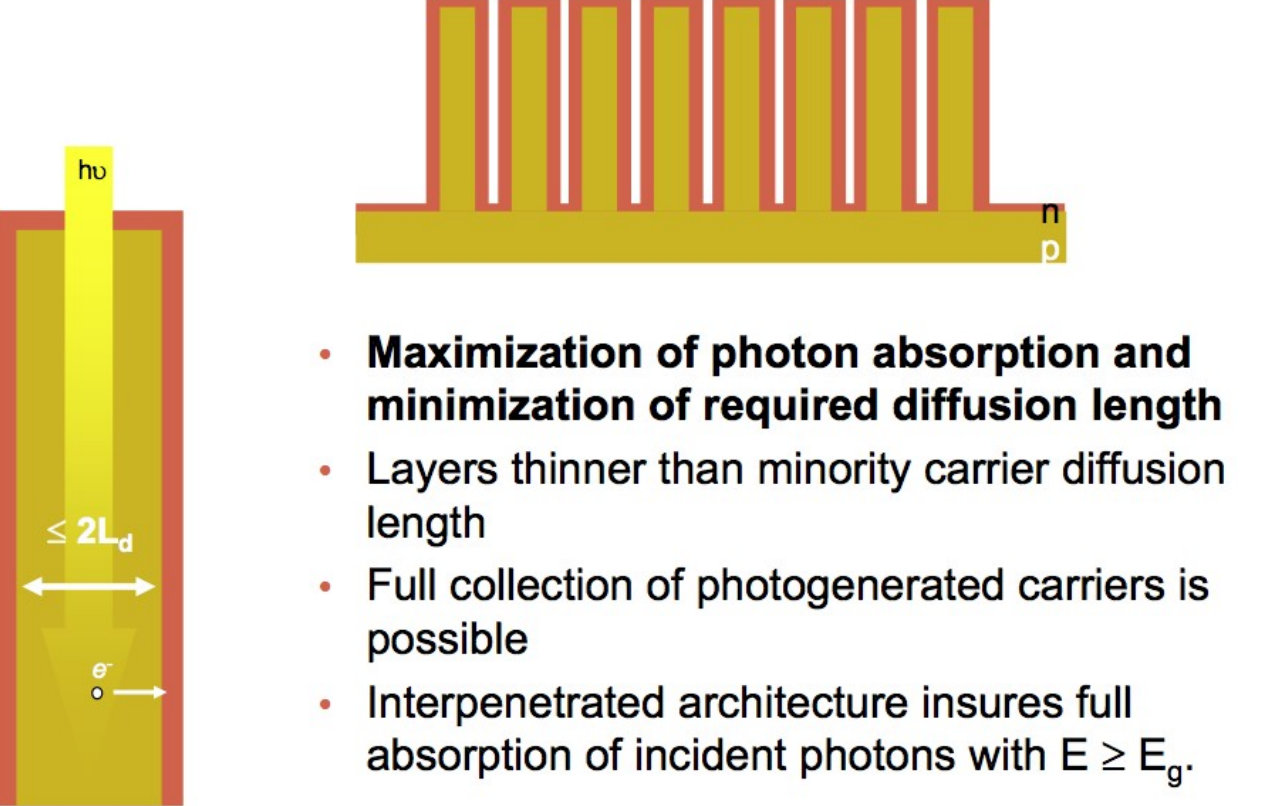
What is the basic design rational of nanostructuring solar cells via vertical arrays with right dimensions vs. traditional different horizontal layers?
to decouple solar adsorption and carrier diffusion
to maximize photon absorption & minimize diffusion length
(often requires enough thickness for effective solar adsorption)
(usually requires small/thin layers for minimized carrier recombination).
What are key advantages of nanodome/nanocone structured Si solar cells?
efficiently reduce reflection and enhance absorption over a broad spectral range
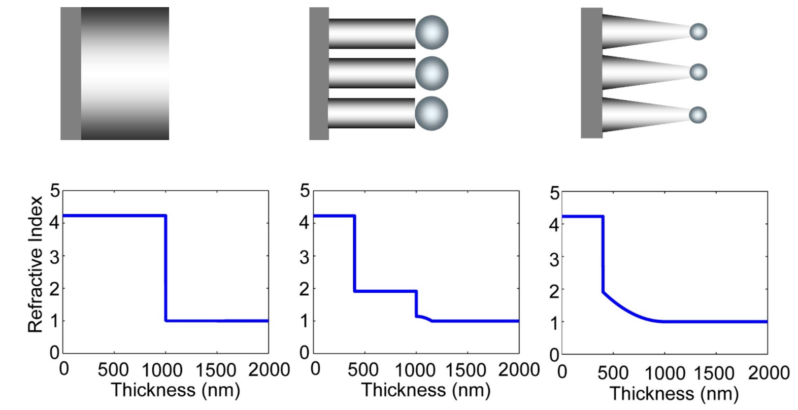
Which has lowest reflection?
case c
Why can graded reflection index help decrease the surface reflection?(lecture 6)
larger changes in N cause reflection
Advantages of III-V Solar cells (4)
Direct band gap materials
Tunable bandgap and lattice---multi-layer solar cell
Well-developed deposition methods
Less temperature sensitive compared with Si
differences between CIGS and CZTS solar cells?
both: thin film solar cell absorber
CZTS made of abundant, cheap, non-toxic
However has high defects or recombination at grain boundaries (worse performance)
Why printed organic solar cell?
its potential for Roll-to-roll printing and processing technologies, which offer high throughput, as well as cost-efficient methods for manufacturing flexible organic devices (already applied for light emitting diodes (OLEDs).
What are the advantages/disadvantages compared with printed inorganic solar cell?
structural flexibility
processing advantages: organic molecular structures and chemical group functionalization (allowing different solvents, concentration tuning, potentially more cost-effective and scalable).
What is the difference between HOMO/LUMO and Valence/Conduction band?
HOMO/LUMO are discrete energy levels associated with individual molecules
while valence/conduction bands are continuous energy ranges in bulk materials with periodic structures.
Usually homo/lumo is better accuracy
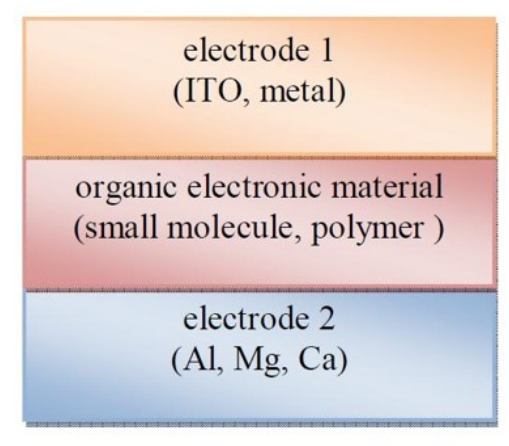
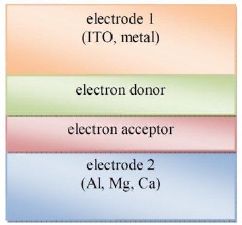
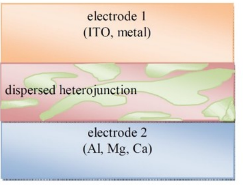
What are the three types of organic solar cells?
Single Layer
Bi-layer structed
Bulk heterojunction
Single layer schematic
Bi-layer structured D-A schematic
Bulk Heterojunction
What is the typical thickness of Donor/Acceptor blend layer (or called active layer)?
100-250 nm.
Why is the thickness for organic-based much smaller than other types of solar cells (for example, Si ~ micrometer thick or up)?
Due to its much higher light absorption efficiency and resulting high optical density, organic D/A active layer has much better light absorption property than inorganic counterparts such as Si, only ~100-250 nm is needed.
typical mobility of organic semiconductors
10^-8 ~10^-1 cm2 /V-s
mobility of organic semiconductors are typically much lower than those for inorganic semiconductors, how can one achieve effective charge separation in organic solar cells?
it is critical design nanoscale phase separated length (in the order of ~10 nm) for bulk heterojunction (BHJ) solar cells, to minimize recombination rate. *
Possible control can be done by processing conditions, such as choice of solvent, blend ratio, annealing time/temperature, etc.
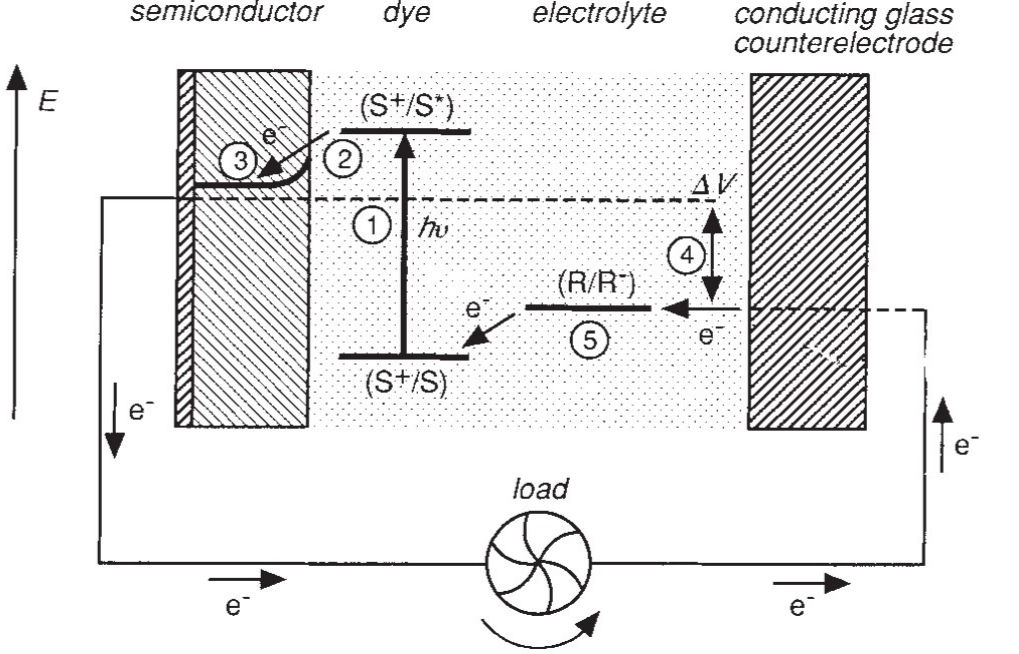
Please draw a simple scheme to show the basic working principle of a dye-sensitized solar cell (DSSC)?
(DSSC) What are key components involved? List several approaches to improve DSSC efficiency? (5)
1. Nanostructured semiconductor anodes;
2. Exploring new dye;
3. New electrolyte or energy relay dye;
4. New mediator;
5. Improving light trapping, e.g. by nanostructuring to employ plasmonics effect. Please refer to the lecture notes.
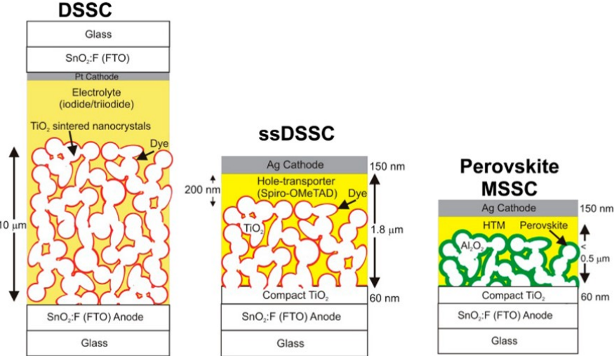
compare the emerging perovskite solar cells with dye-sensitized solar cells. What is the main fundamental reason that perovskite solar cells have a boost efficiency over DSSC?
superior charge transport and collection
bandgap tunable from 1.5 to 2.2. eV
perovskites have better adsorption efficiency, simpler processing
charge separation occurs in perovskite
Perovskite had charge transport layers vs semiconductor and electrolyte
Con: stability due to ion migration
Dssc:
relies on dye regeneration process and the electrolyte.
What are several key fundamental steps for water splitting?
Schematic for water splitting
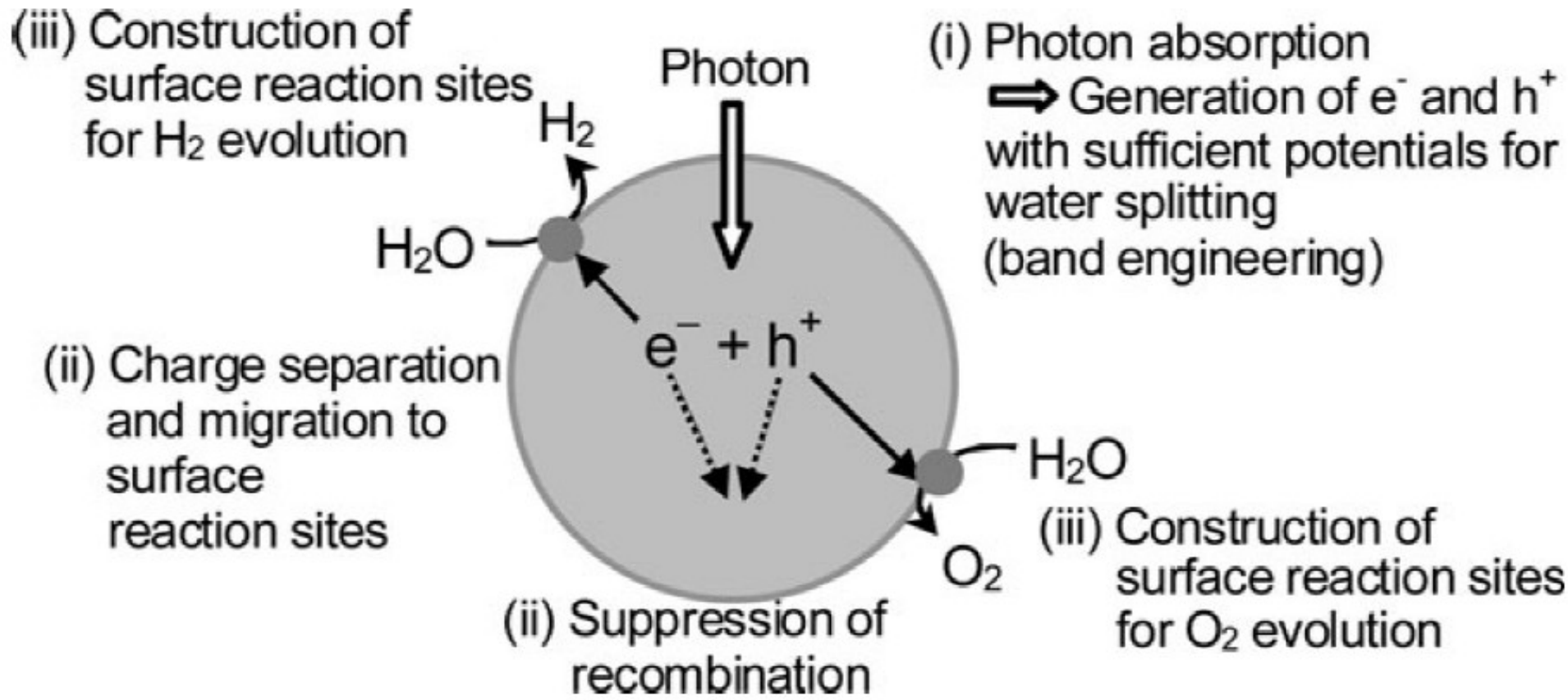
Key steps for water splitting
1) Absorption of photons to form electron-hole pairs.
2) Charge separation and migration of photogenerated carriers.
3) Surface chemical reactions.
Surface Chemical reaction of Water Splitting
surface character (active sites)
quantity (surface area).
Even if the photogenerated electrons and holes possess thermodynamically sufficient potentials for water splitting, they will have to recombine with each other if the active sites for redox reactions do not exist on the surface.
Charge separation and migration of photogenerated carriers in Water Splitting
(Crystal structure, crystallinity and particle size strongly affect the step)
absorption of photons in water splitting
semiconductor photocatalyst materials is the width of the band gap and levels of the conduction and valence bands (band engineering);
Three key material challenges (the ‘Big three’) for achieving optimal water splitting:
1. Efficiency: right materials that have bang gap Ebg ~1.6-2.2 eV (right band gap and band position Ecb and Evb), and have high photon-to-electron conversion efficiency;
2. Stability/Durability: semiconductor materials need to be stable in aqueous solution;
3. Energetics: band edges for semiconductors need to straddle H2O redox potentials (HER and OER).
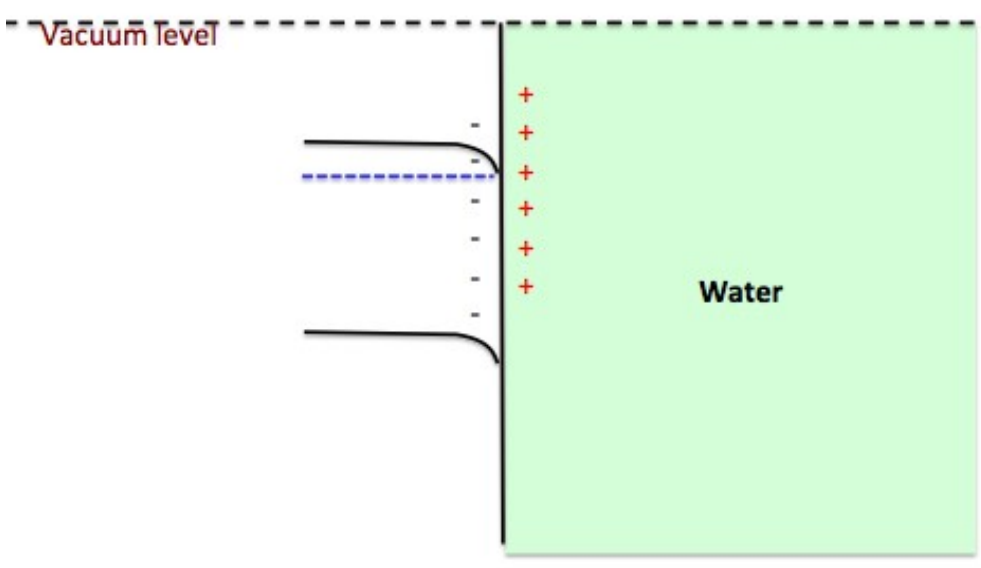
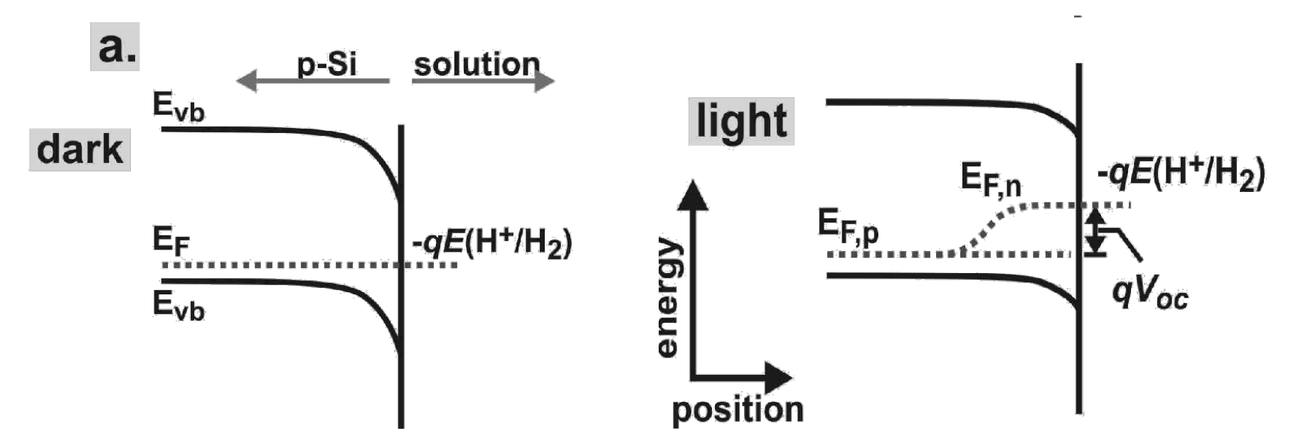
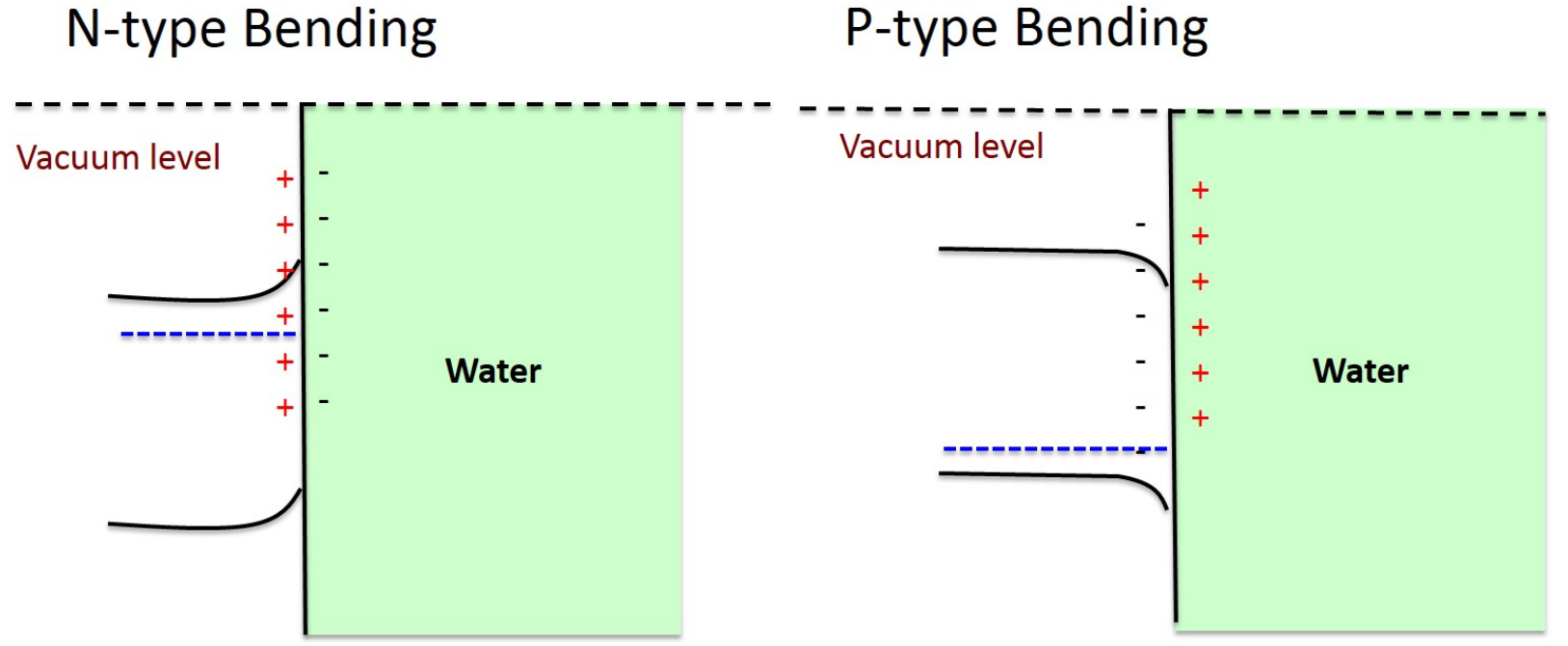
From band bending point of view, what is wrong for the following figure? And why? Explain why p-type Si can be used as photocathode.
p-Si (p-doped) can be used as photocathode for Hydrogen Evolution Reaction (HER), see below for its band bending mechanism
The correct schemes for N- and P-type bending
five types of integrated photoelectrochemical PEC devices
single semiconductor
double semiconductor
integrated pv-pec
buried pv electrolyzer combined
tandem water splitting device
Features of Tandem Water Splitting Device (4)
1) Maximize light absoprtion of solar spectrum by employing two semiconductor materials (photocathode and photoanode separately) with different band gaps
2) Vertical Nanowire/rod array electrodes can decouple light absorption and carrier separation to minimize surface recombination, for efficiency enhancement.
3) Molecular catalysis loaded on each nanowire/nanorod electrode can efficiently catalyze the surface chemical reaction.
4) Using proton (H+) transport membrane will selectively allow only proton across the membrance, effectively separate H2 and O2.
Purpose of Phonon Glass Electon crystal:
PGEC: phonon glass & electron crystal is to maximize the figure of merit for TE materials ((high σ, electronic conductivity; low κ, thermal conductivity)
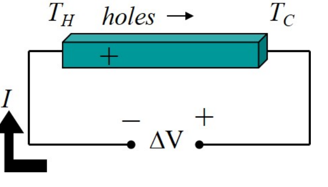
Please explain why the Seebeck Coefficient is positive in p-type semiconductor, and negative in n-type semiconductor?
For p-type, the major carrier is holes, which under thermal gradient will be driven from TH to TC. Therefore for p-type, S is positive. Vice versa for n-type (negative S)
S = -DeltaV/DeltaT
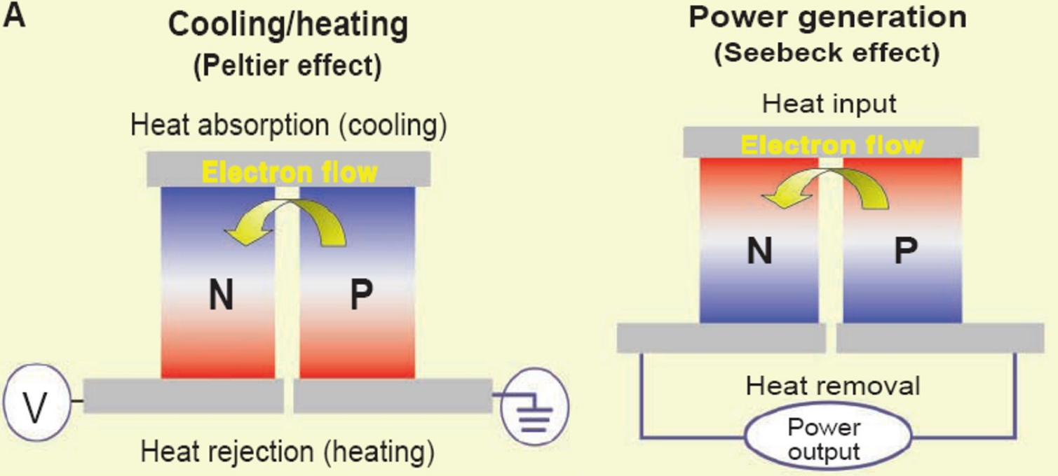
Please use a diagram to explain the similarity and difference between a refrigeration mode and power-generation mode based on thermoelectric
What is the typical value range for ZT materials?
0.5~1.0 (advanced nanomaterials developed in lab has the reported values up to ~3.0). ZT values have temperature dependence!
What are the strategies to improve the values of TE?
‘Nano approach’ by nanostructuring existing known TE materials, and developing totally new TE materials.
‘low dimensional control’, leading to higher density of state (α increases),
enhanced phonon scattering (effectively lowering κ), and
enhanced carrier mobility (σ increases)
solar spectrum
Ultraviolet (UV): Photons with energies roughly from 3 eV to 124 eV.
Visible: Photons with energies from roughly 1.8 eV (red) to 3 eV (violet).
Infrared (IR): Photons with energies from roughly 0.001 eV to 1.8 eV.
Shockley-Queisser limit
Shockley-Queisser limit describes the maximum theoretical efficiency of a single-junction solar cell, about 33.7%, due to unavoidable losses like heat generation and light reflecting off the surface.
Amorphous vs Crystalline Si
amorphous is unstable but straps more light, cheap
crystalline is indirect bandgap and needs thicker films, higher efficiency
2 mechanisms of thermoelectrics
seeback
peltier
Seebeck vs peltier
Seebeck converts heat to electricity, while Peltier converts electricity to heating or cooling. They are both manifestations of how charge carriers move in response to temperature gradients
CTEG or (TEC) (peltier) vs Cooling (vapor compression)
Peltier:
smaller
lower efficiecy
quiet
higher cost