ECE Lab 2, 3, 4, 5 & 6: Op-Amps I & II, Filters I & II, Diode Circuits
1/35
Earn XP
Description and Tags
Name | Mastery | Learn | Test | Matching | Spaced | Call with Kai |
|---|
No analytics yet
Send a link to your students to track their progress
36 Terms
Operational amplifier as a Comparator
Active device: capable of supplying energy to a circuit.
Needs external power supply.
Can modify/ amplify circuit.
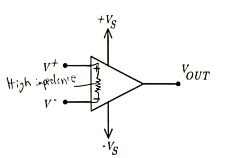
High input impedance
Little current in/out of V+ and V- pins.
Doesn’t present load on preceding circuit elements.
Low output impedance.
Source/ sink current from output → provide output to next elements
Provide Buffering or Isolation b/w circuits
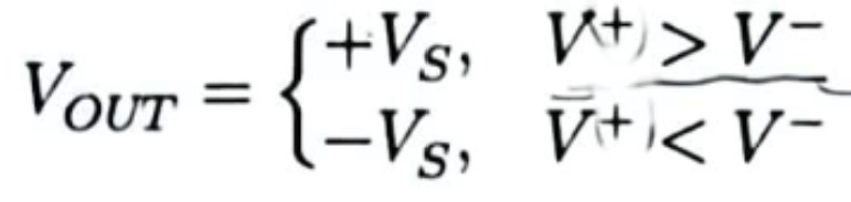
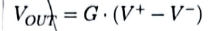
Op-amp Open-Loop Gain
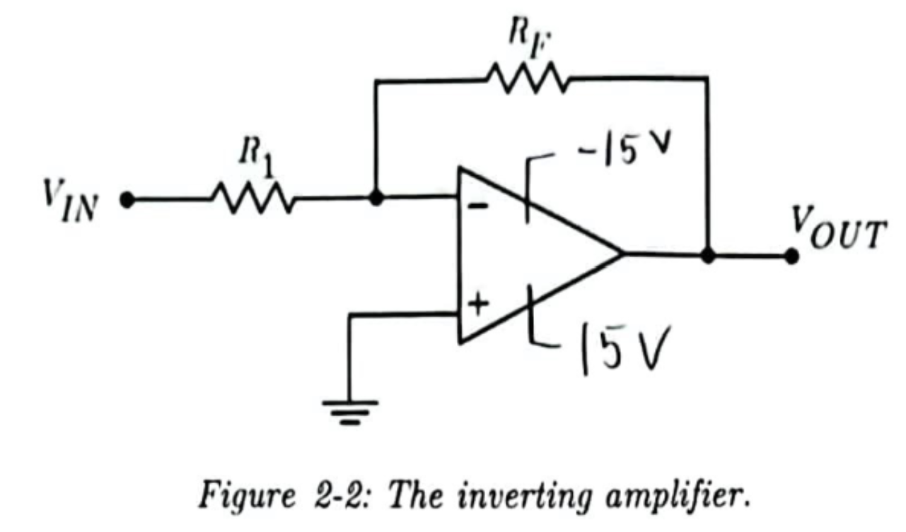
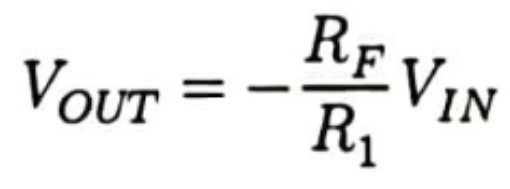
Inverting Amplifier
Op-amp with negative feedback.
Multiplies the input voltage by a negative gain, producing an output signal that is 180∘ out of phase with the input
180 Degree Phase shift = multiplying by factor of -1
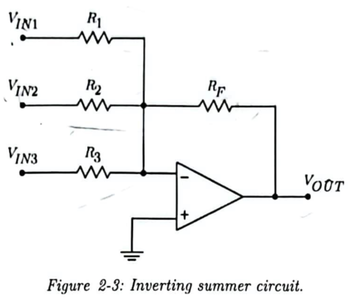
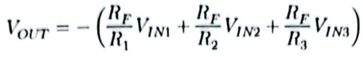
Inverting Summer
Three inputs
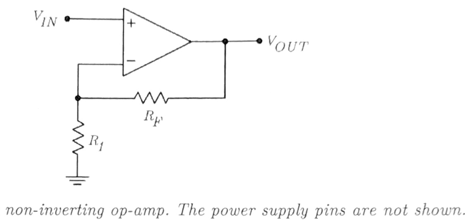
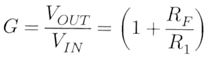
Non-Inverting Op-amp
Amplifies input voltage without phase shift.
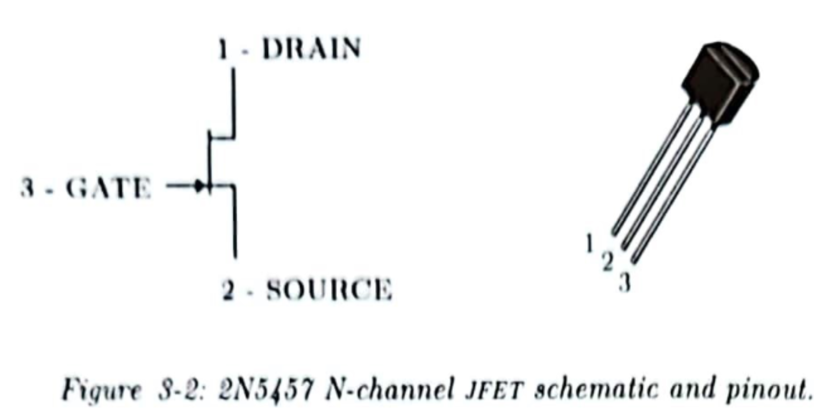
JFET as a variable resistor
Voltage-controlled resisstor
As V_c goes from 0V → V_th
R_th goes to inffinity
Filter
The fundamental purpose is to change the magnitude and phase of the sinusoidal components of an input signal.
Filtering
Manipulating Periodic Signals based on their frequency content.
Periodic signal - Fourier’s theorem
A periodic signal may be represented by a sum of sinusoidal components.
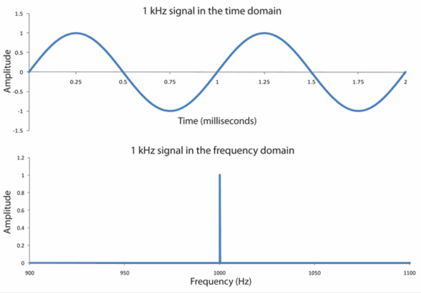
Frequency Domain and Sine waveform
Voltage vs. Frequency
Plot of the magnitude of sinusoidal components vs. their frequency.
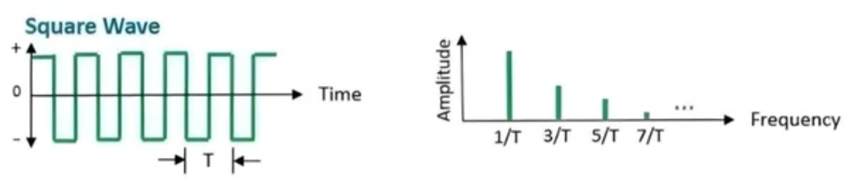
A pure sinusoid has all signal power concentrated at a single frequency component (a delta function). Amplitude = V_pp / 2
FFT - Fast Fourier Transform analyzes a signal's time-domain waveform and converts it into the frequency domain.
Square Waveform
Amplitude = 4 / π n
(n = 1 for the fundamental frequency)
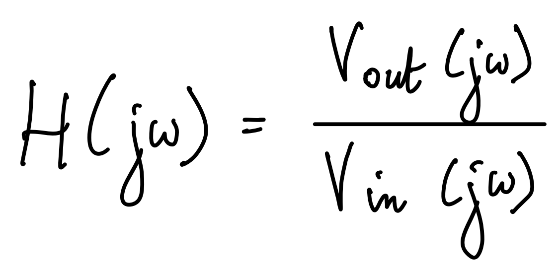
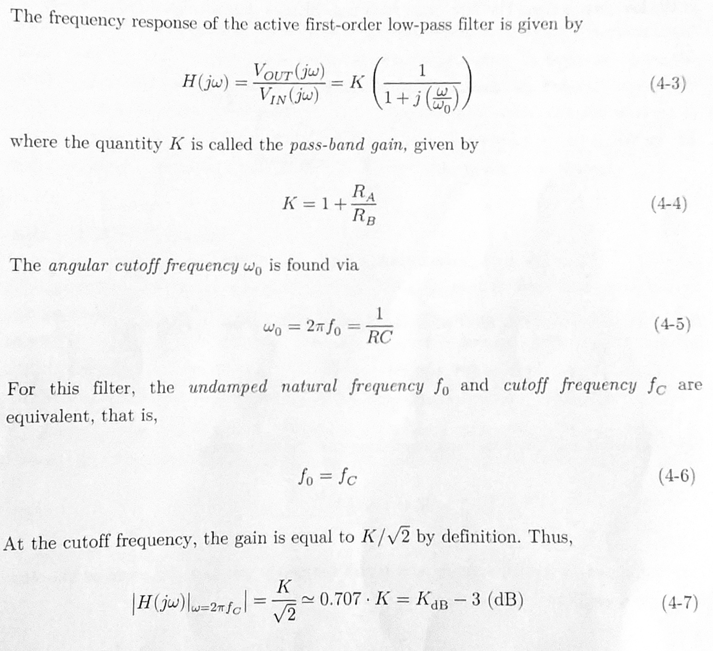
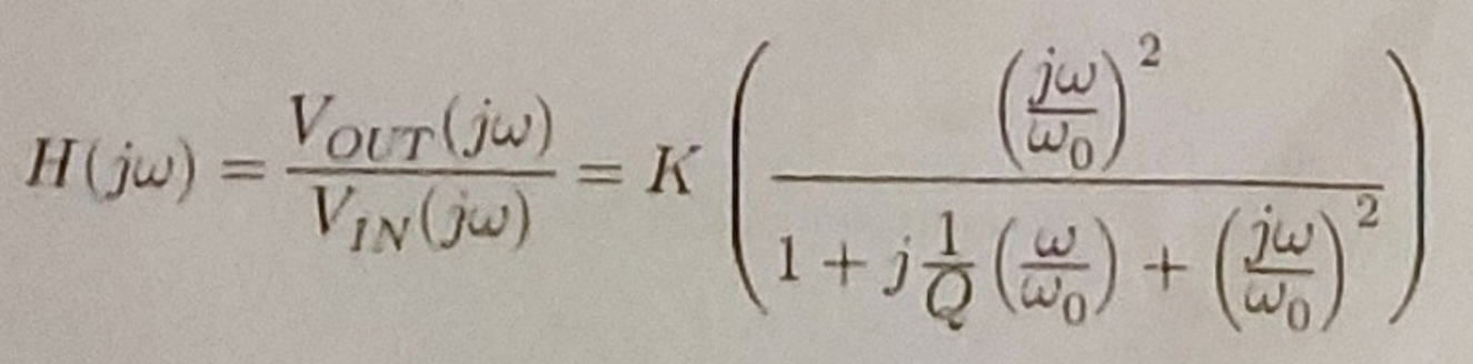
Frequency Response H(jω)
ω = 2 π f
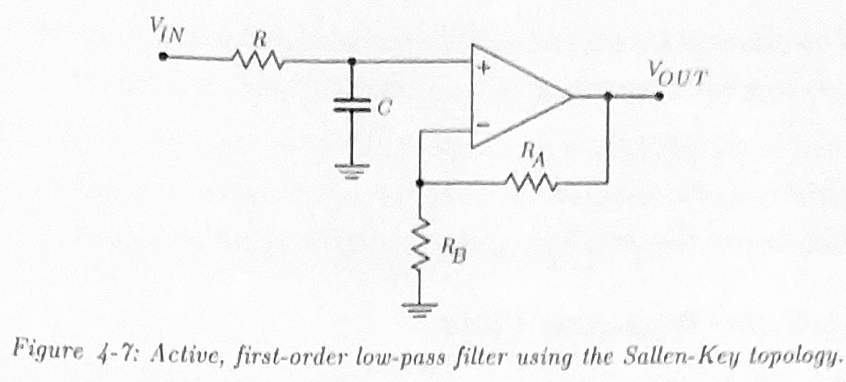
Active first-order low-pass filter
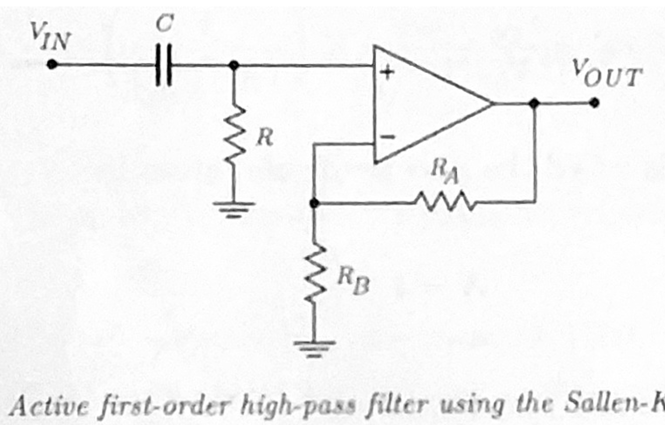
Active first-order high-pass filter
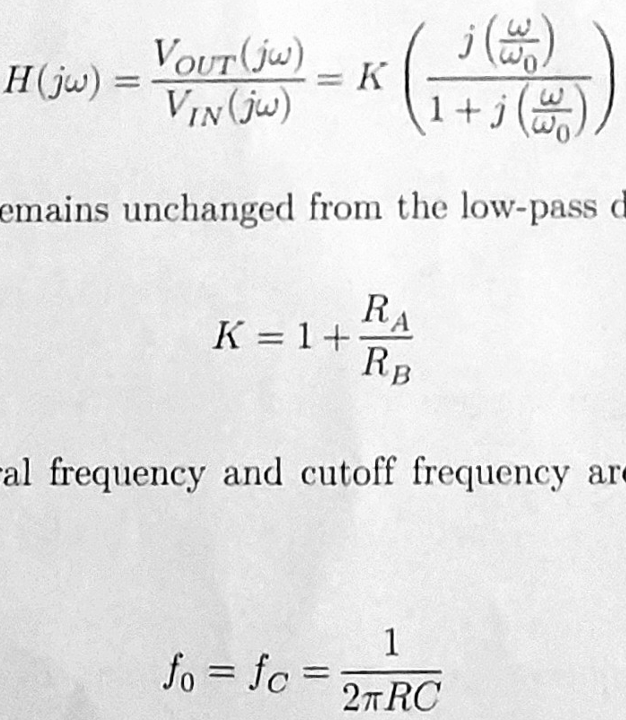
Advantage of active filter
Property of Op-amp making it possible
Allows us to add a load without changing gain
It isolates the load resistor
Active second-order low-pass filter
Provide improved performance in signal processing.
f_c = x f_0
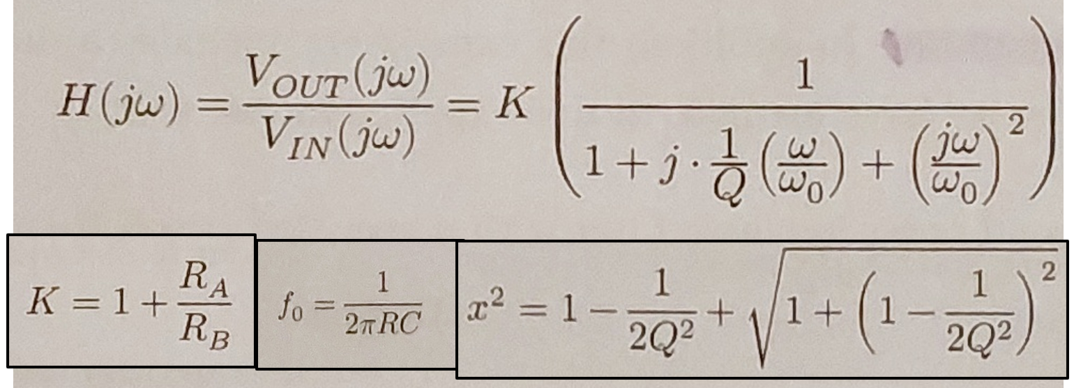
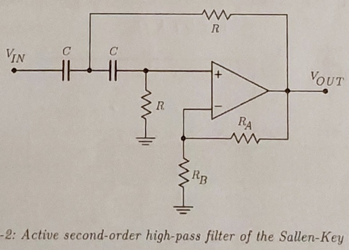
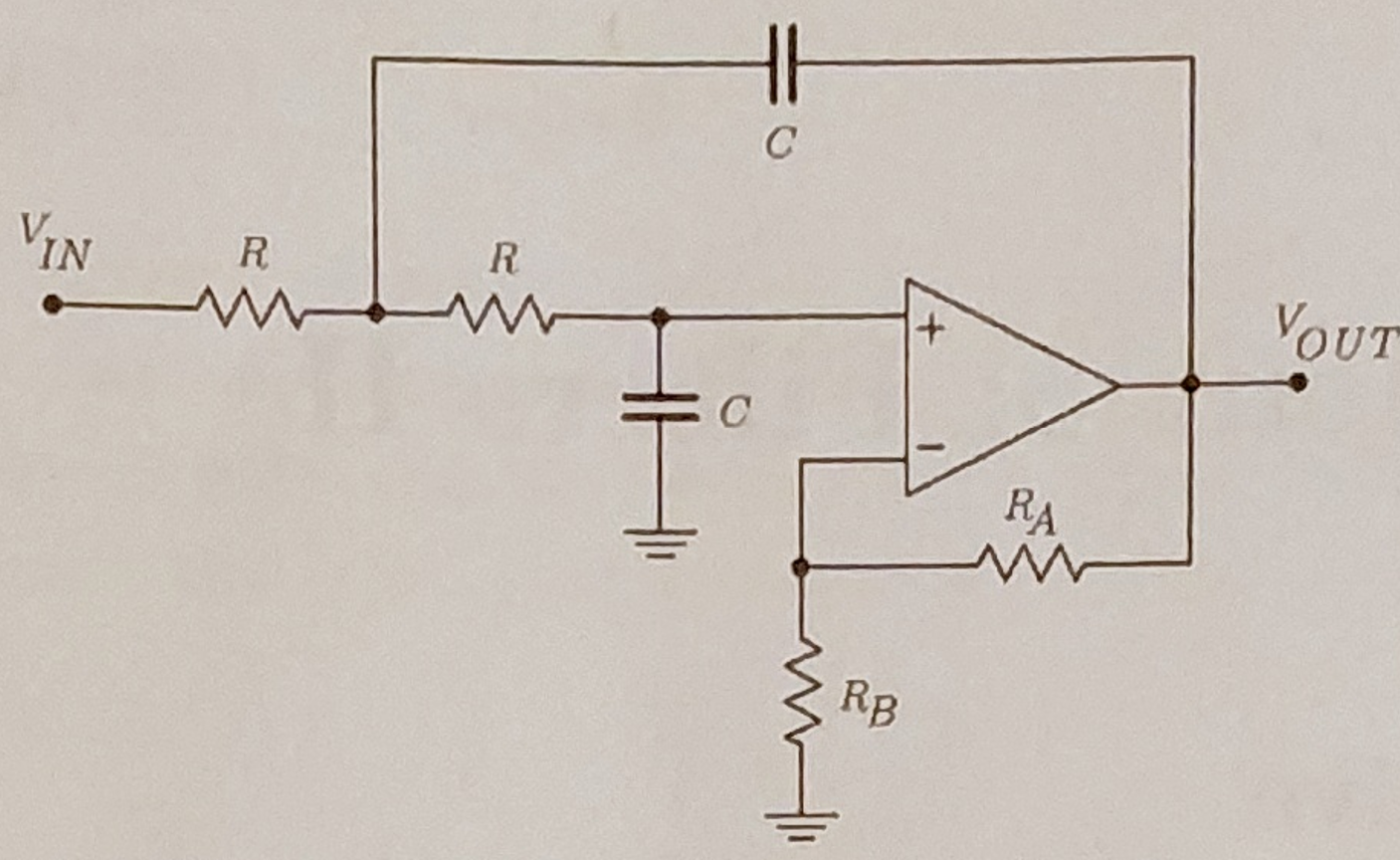
Active second-order high-pass filter
f_c = x f_0
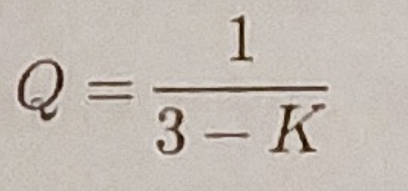
Quality Factor
Influences Shape of the frequency response
Increasing Q leads to a sharper/ narrower peak near the resonant frequency and a higher peak Gain
Critically Damped: Q = 1/sqrt(2) and f_c = f_0
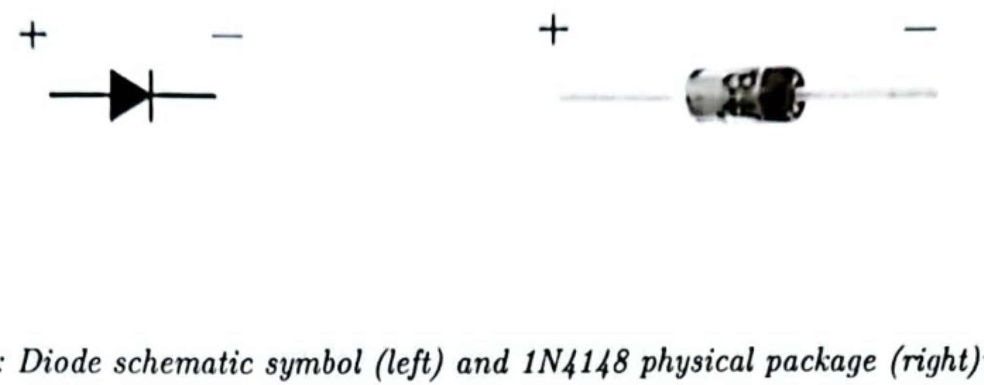
Diode
Two terminal circuit element that has polarity, current can only flow in one direction.
Forward Bias: 0.6V IDEALLY 0V (acts as a wire)
Reverse Bias: OPEN
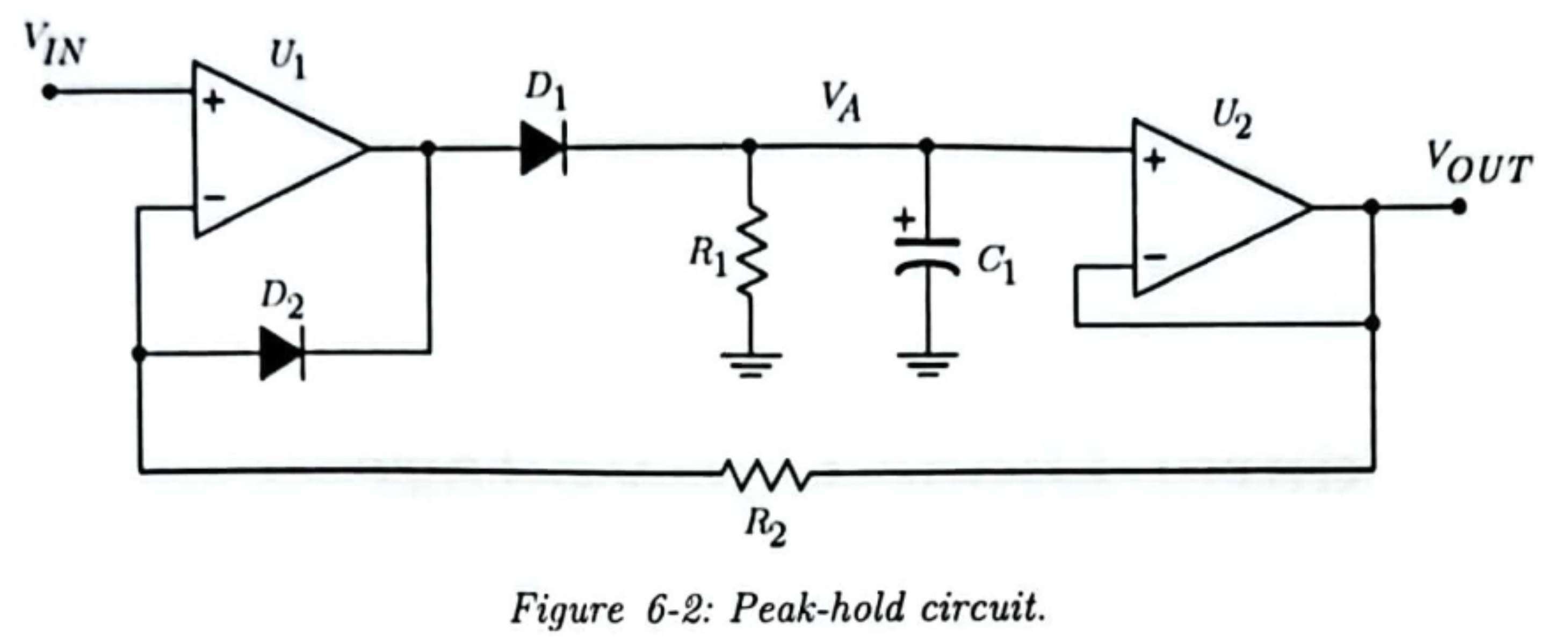
Peak-Hold Circuit / Peak detector circuit
Monitors positive/ negative peak of an input signal.
V_OUT = V_IN when the input signal is increasing.
If the input signal drops below the peak value the output will hold.
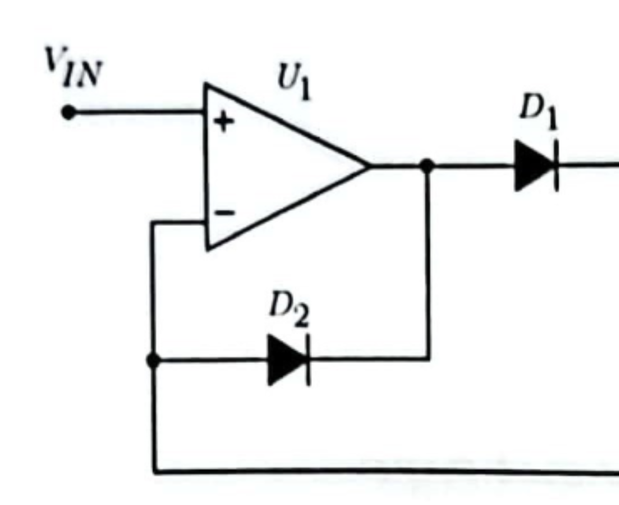
Diode Input Stage (non-linear) → (U1, D1, D2)
Voltage follows the input as it increase
If V_IN drops below peak, Diode 1 will reverse bias preventing V_A from dropping
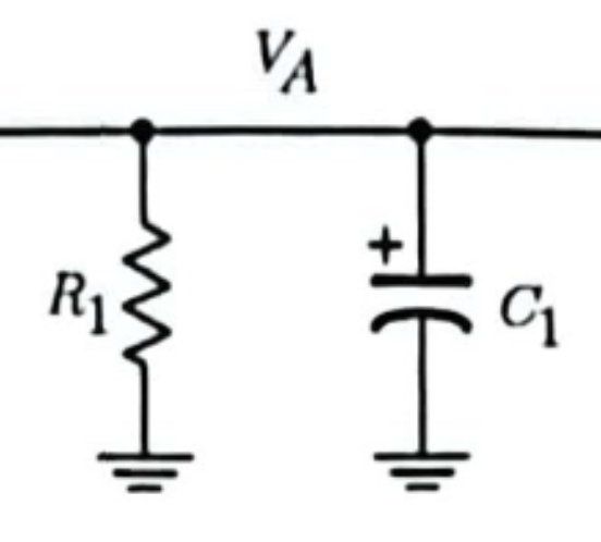
Stage 2 → (R1, C1)
The capacitor (C1) holds the peak voltage by storing charge.
The resistor (R1) provides a discharge path to ground.
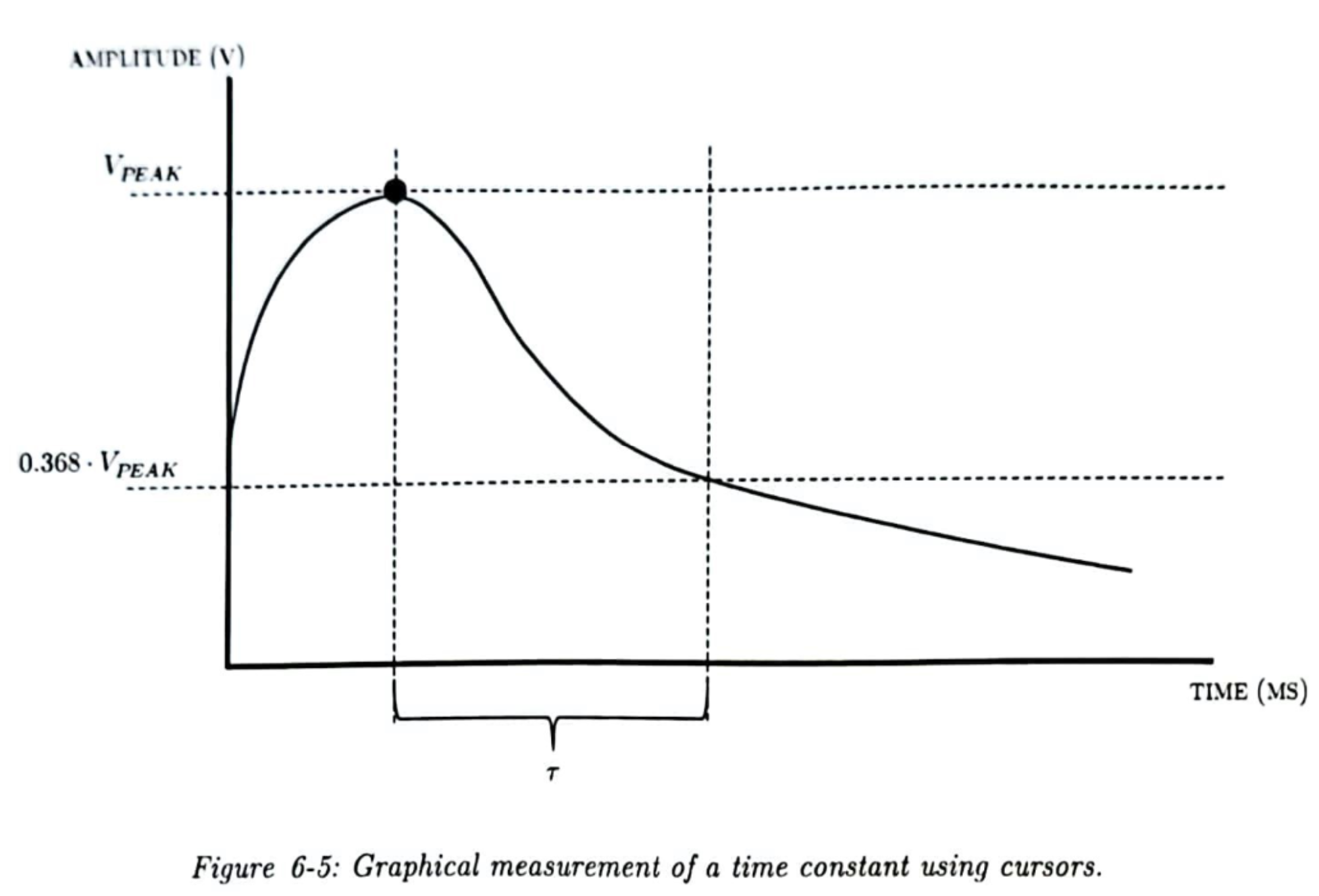
Time Constant
Amount of time it takes the output to decay by a factor of 1/e = 0.368
t = R1C1
Voltage Follower Stage → (U2)
Buffer that prevents the scope from loading and prematurely discharging the capacitor.
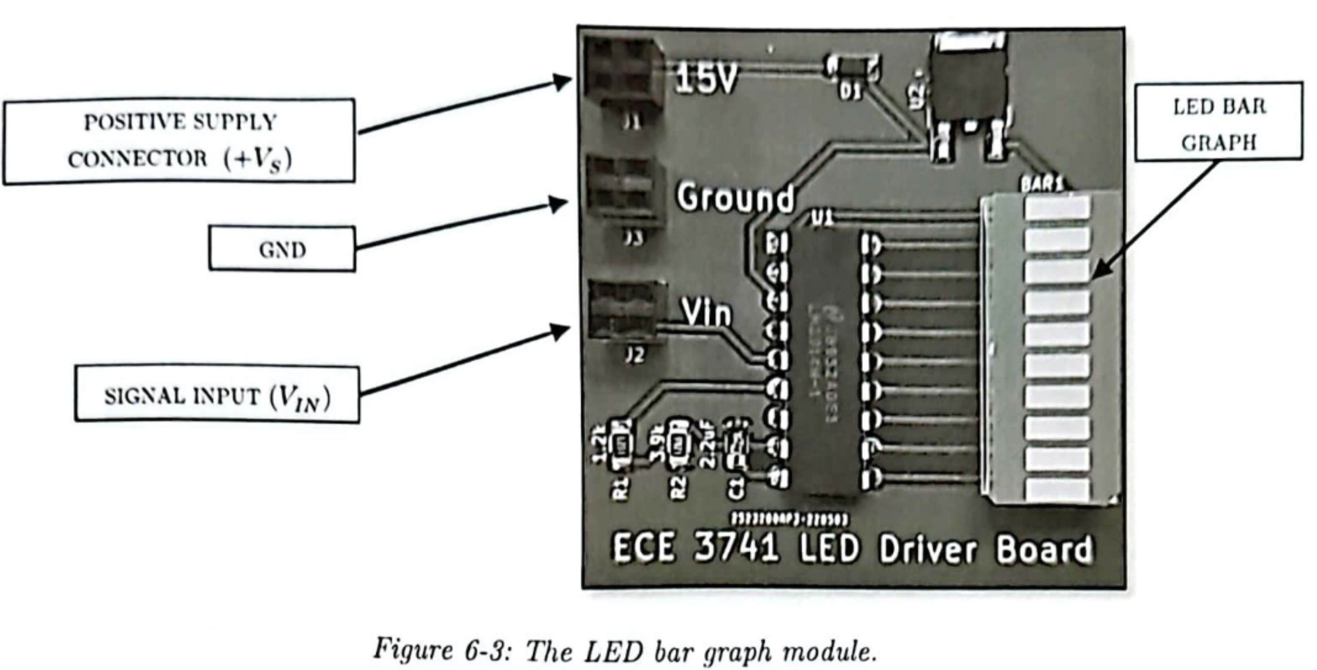
LED Graph Bar module
Allows us to illuminate a sequence of 10 LEDs in proportion to a single input voltage.
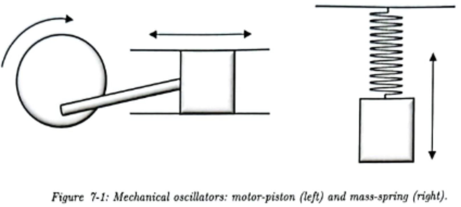
Oscillator Circuit
Produces a periodic output signal without any applied input signal
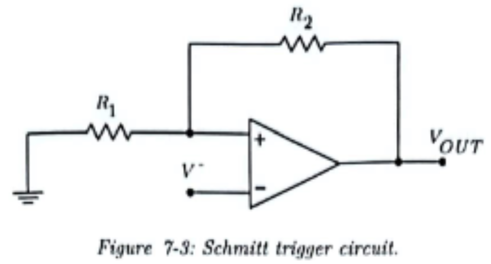
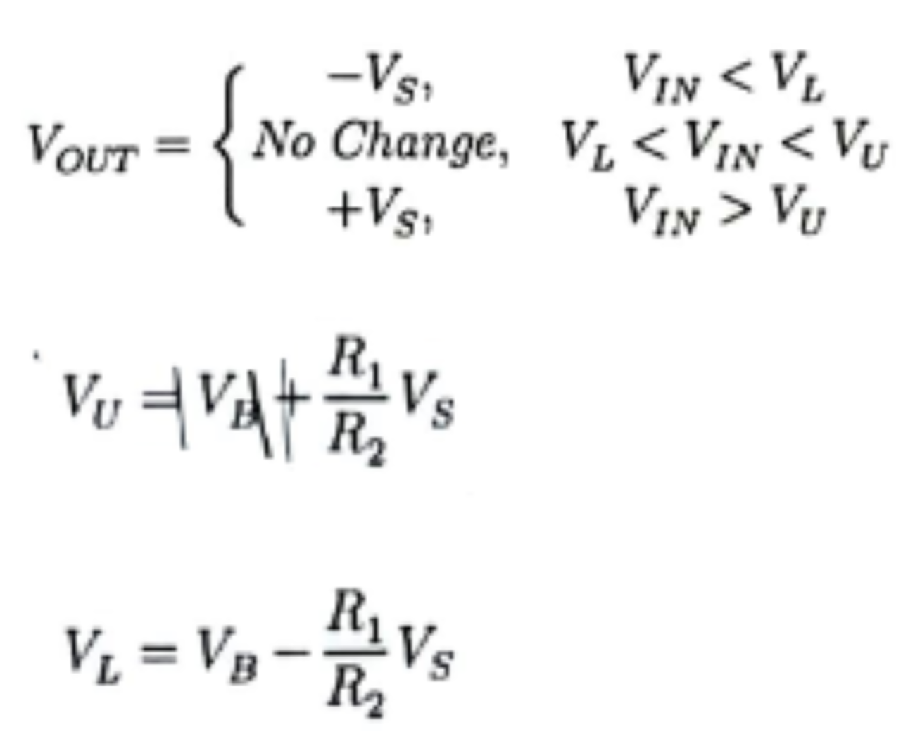
Schmitt trigger circuit
Comparator + Positive feedback = Hysterisis (2 thresholds)
"memory" effect makes the circuit less sensitive to noise.
Used to convert a noisy input signal into a clean digital output.
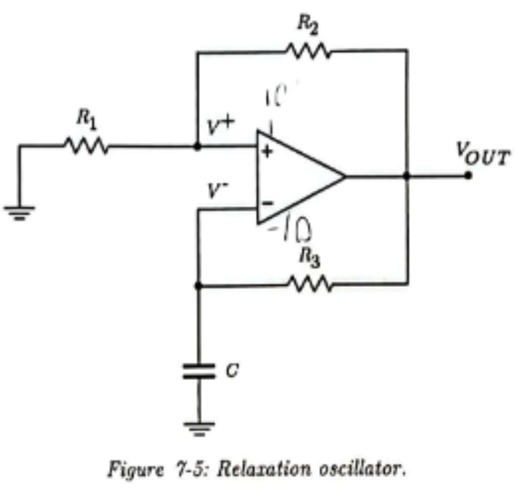
Relaxation Oscillator
Schmitt Trigger + RC Circuit
R1, R2, R3 and C all determine the frequency of the oscillation
Square waves
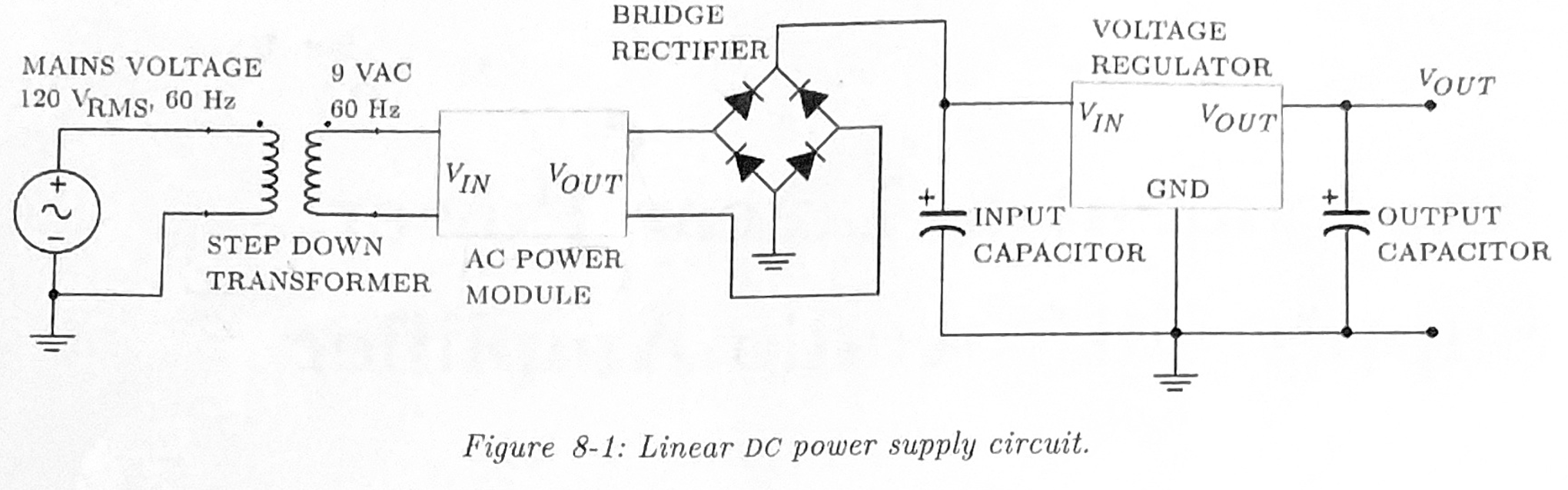
Linear DC Power Supply Circuit
Mains Voltage (120 VAC, 60 Hz) Standard Wall Outlet
Step Down Transformer Wall Wart: Steps down 120VAC to safer 9 VAC, 60 Hz.
Bridge Rectifier: 4 diodes to convert the bipolar AC sine wave into a unipolar (positive only), 9 VAC,120 Hz Doubling the number of peaks per second.
Filter Capacitor: Smoothens the pulsating DC into a "ripply" DC voltage by storing charge and releasing it between the peaks.
Voltage Regulator: Rremoves nearly all the remaining ripple to produce a clean, stable DC output.
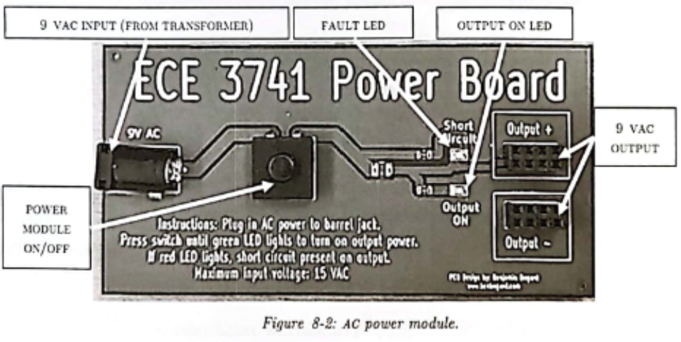
AC Power module
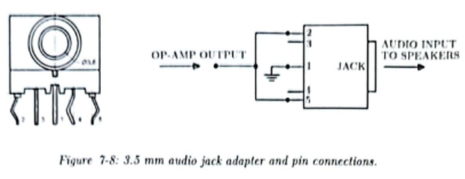
mm audio jack adapter and pin comnnections
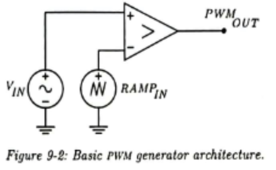
Pulse Width Modulation
A pulse width modulation signal encodes information in the width of a train of regularly spaced square pulses.
NOt Amplitude.
Used in Motor control, Analog to discrete conversion and voltage regulators.
Sample rate: frequency at reach sample is taken
Either “low” or “high”
The higher the input amplitude, the longer the PWM is high
Duty Cycle: Percent of time PWM is high for a sample period
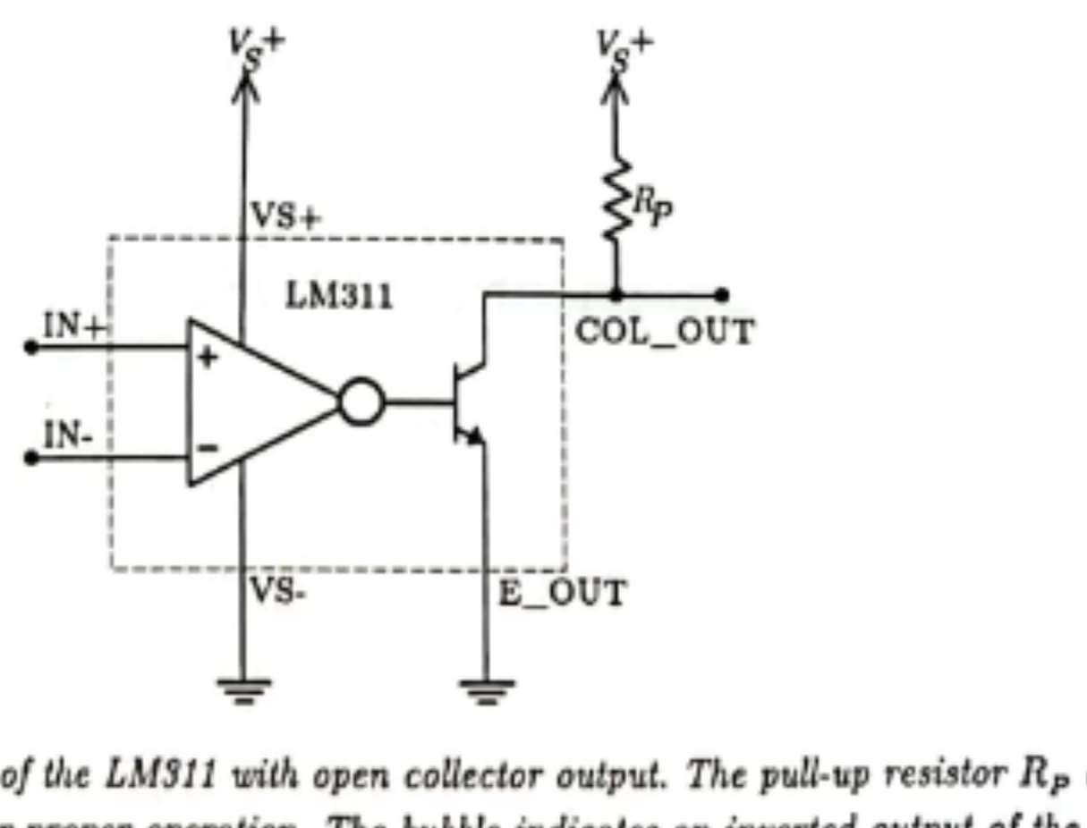
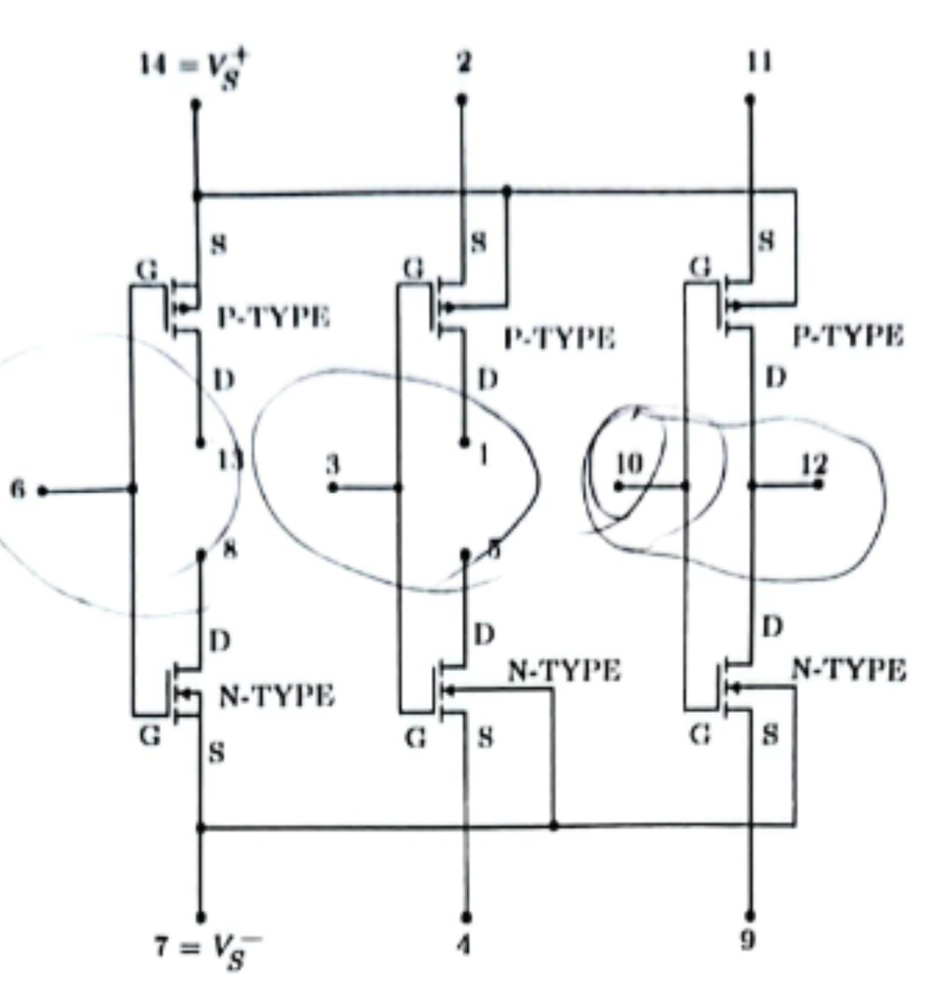
LM311 Comparator
Not Op-amp
Open collector output: Can’t output supply voltages on its own
Pull-up Resistor R_p well defines COL_OUT terminal as +Vs
Pulls up PWM output so it doesn’t float/ fall flat.
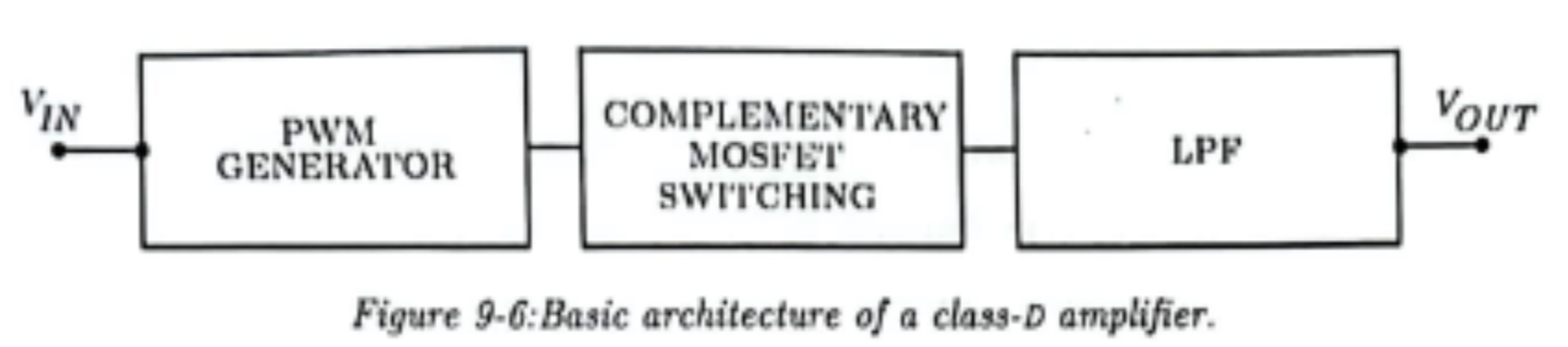
Class-D Amplifiers
Uses Rapid ON/OFF switching of transistors instead of a constant bias current.
G = V_OUT/ V_IN
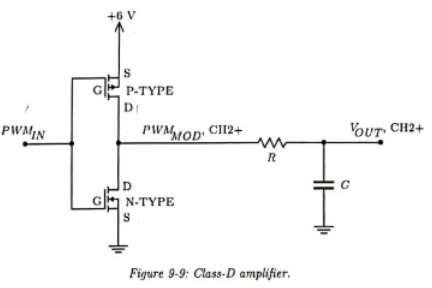
Complementary MOSFET Switching
Logically Invert PWM_IN Signal creating PWM_MOD
Voltage controlled switches
Opposite polarity: when P-MOSFET is on and pulls PWM_MOD to +Vs, N-MOSFET is off
Switches and Sensors
Op-amps: current limited outputs
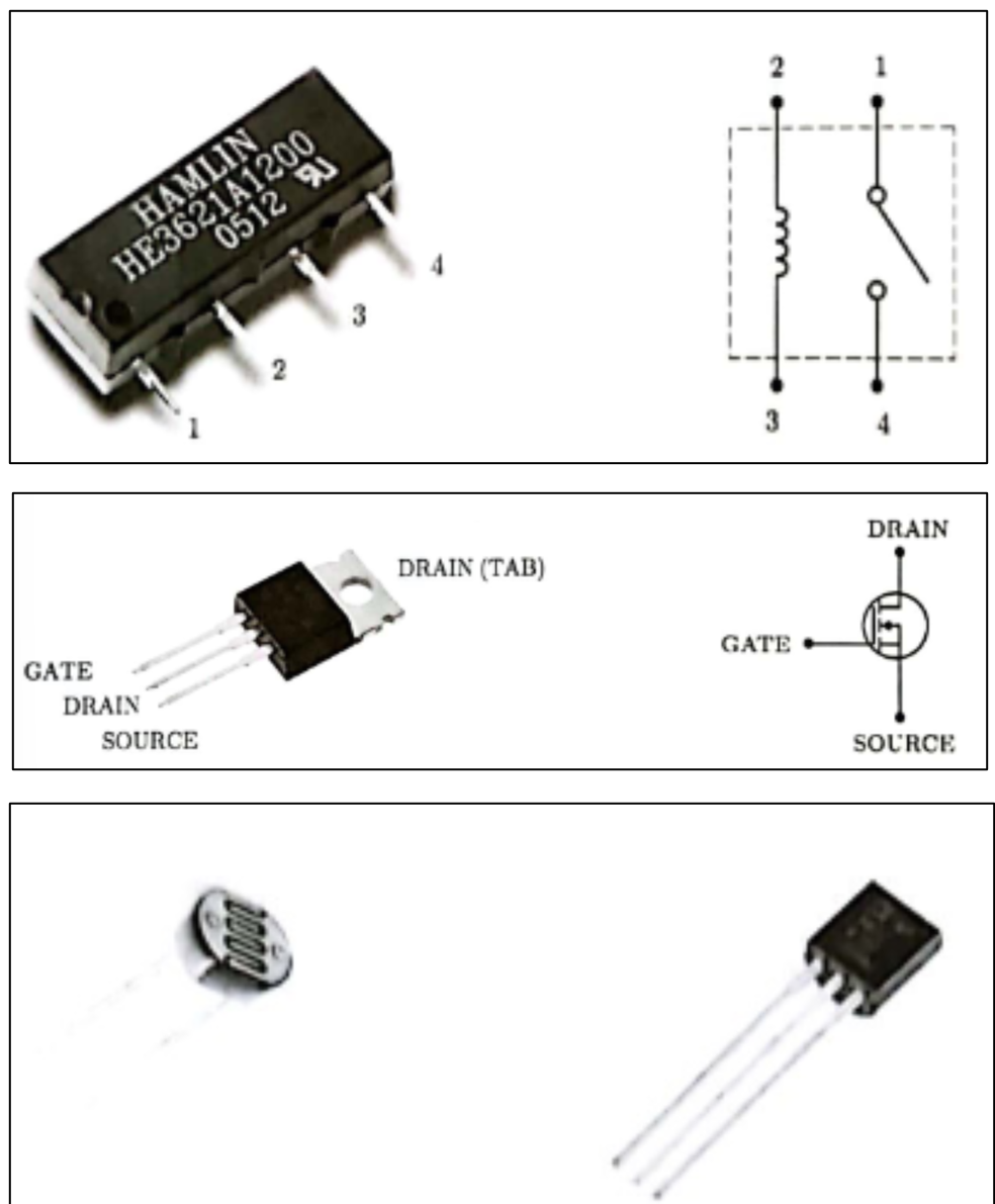
Physical Relay: electromechanical switch normally open
MOSFET: Solid State Voltage controlled switch
Push Button: Physical switch get’s shorted
Schmitt Trigger: “de-bouncing” Hysteresis for clean switching.
Photocell: Resistance increases as light reduces
Temperature sensor voltage increases as temperature increases
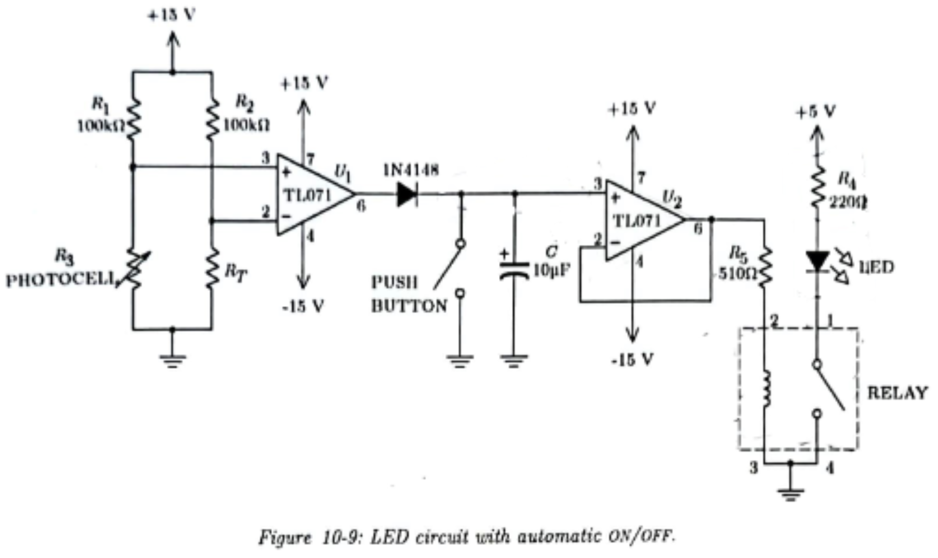
LED circuit with automatic ON/OFF
Light decreases, resistance increases, U1+ increases → +Vs
Capacitor charges, discharges through push button
U2 is a voltage follower, buffer, provides current to relay coil.