Looks like no one added any tags here yet for you.
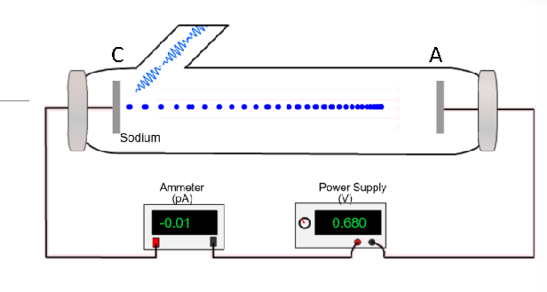
Photoelectric Effect
When light shining on a metal causes electrons to be emitted
Einstein's Prediction
Light comes in tiny packets of energy, and the energy of each packet is related to the frequency of the light
Photoelectric Effect
When light shining on a metal causes electrons to be emitted
Einstein’s Prediction
Light comes in tiny packets of energy, and the energy of each packet is related to the frequency of the light
DETAILED EXPLANATION
Photons transfer their energy to electrons in the metal
One photon gives all its energy to one electron
Electrons emitted directly from the surface have the most energy
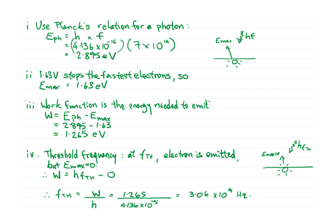
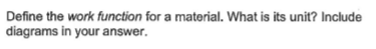
Max energy of emitted electrons depends on the light's freq & metal's work function
Ek = hf - W
Stopping potential (the voltage needed to stop electrons) is measured
Electron energy depends on light freq, not intensity, and that stopping potential increases linearly w/ freq
Validated light is quantised and the energy of a photon is given by E=hf
SIMPLIFIED Explanation
Light Shines on a metal
Causes electrons to be emitted
Stopping Voltage applied to stop the electrons
Stopping Voltage related to kinetic energy of electrons
Varying light freq
Allows us to observe the relationship w/ light freq & electron kinetic energy
Results match Einstein’s Prediction
Electron energy depends on light freq
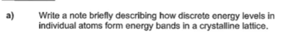
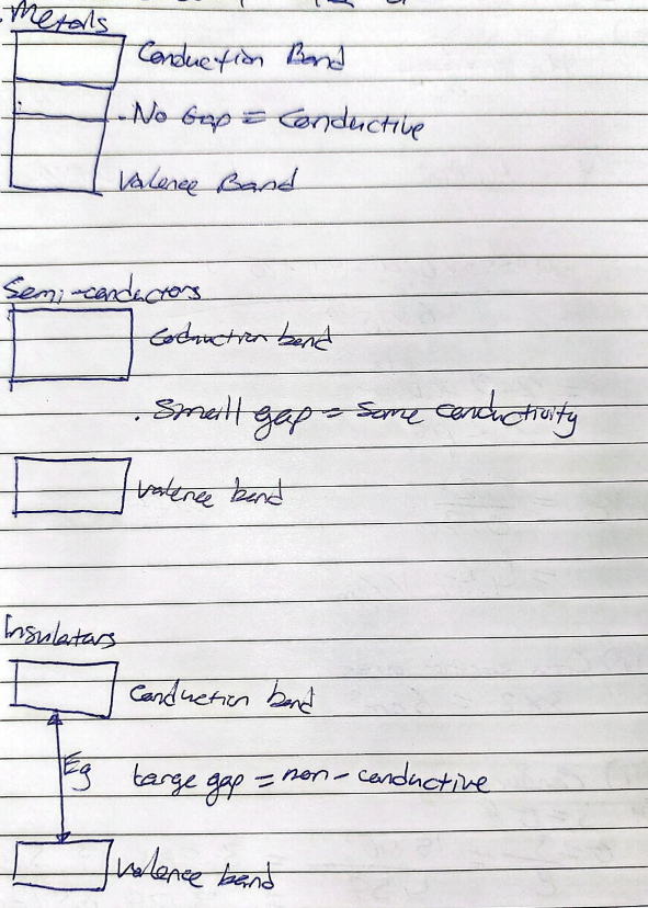
When atoms are far apart, their electrons occupy distinct energy levels
As atoms get closer together, their wave functions begin to overlap
The electron energy levels cannot be the same in the bonded atoms. Thus the discrete energy levels of individual atoms split into a large number of closely spaced energy levels
These closely spaced energy levels form an energy band
e.g. In Si, the 3s & 3p bands merge into a single band, which then splits into the valence and conduction band
Work function for a material:
The min energy needed to remove an electron from the Fermi level at the surface of the material into a vacuum
Unit:
eV or J (electron-volts or joules)
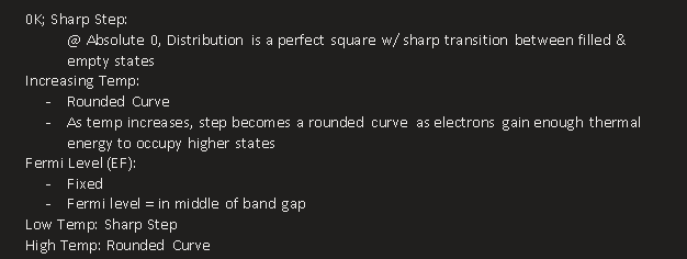
0K; Sharp Step:
@ Absolute 0, Distribution is a perfect square w/ sharp transition between filled & empty states
Increasing Temp:
Rounded Curve
As temp increases, step becomes a rounded curve as electrons gain enough thermal energy to occupy higher states
Fermi Level (EF):
Fixed
Fermi level = in middle of band gap
Low Temp: Sharp Step
High Temp: Rounded Curve
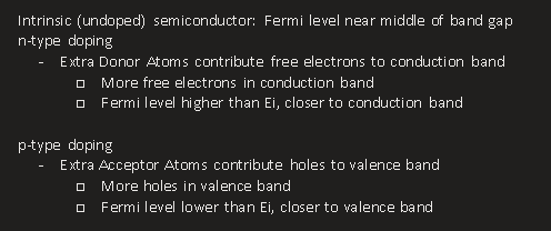
Intrinsic (undoped) semiconductor: Fermi level near middle of band gap
n-type doping
Extra Donor Atoms contribute free electrons to conduction band
More free electrons in conduction band
Fermi level higher than Ei, closer to conduction band
p-type doping
Extra Acceptor Atoms contribute holes to valence band
More holes in valence band
Fermi level lower than Ei, closer to valence band
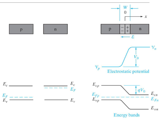
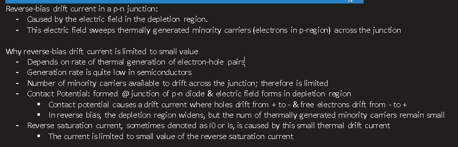
Reverse-bias drift current in a p-n junction:
Caused by the electric field in the depletion region.
This electric field sweeps thermally generated minority carriers (electrons in p-region) across the junction
Why reverse-bias drift current is limited to small value
Depends on rate of thermal generation of electron-hole pairs
Generation rate is quite low in semiconductors
Number of minority carriers available to drift across the junction; therefore is limited
Contact Potential: formed @ junction of p-n diode & electric field forms in depletion region
Contact potential causes a drift current where holes drift from + to - & free electrons drift from - to +
In reverse bias, the depletion region widens, but the num of thermally generated minority carriers remain small
Reverse saturation current, sometimes denoted as I0 or Is, is caused by this small thermal drift current
The current is limited to small value of the reverse saturation current
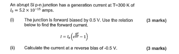
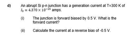
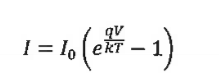
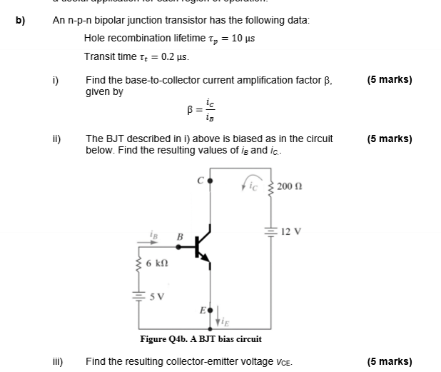
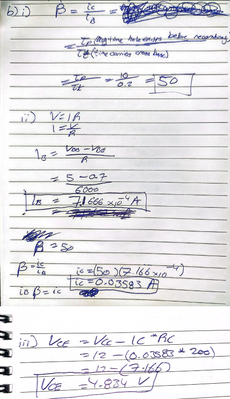
i)
Put the given I0, q, V, k, T into the formula
ii)
Same as i) but -0.5V
Values not the same but same method
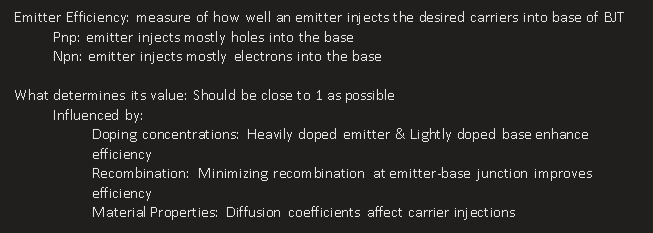
Emitter Efficiency: measure of how well an emitter injects the desired carriers into base of BJT
Pnp: emitter injects mostly holes into the base
Npn: emitter injects mostly electrons into the base
What determines its value: Should be close to 1 as possible
Influenced by:
Doping concentrations: Heavily doped emitter & Lightly doped base enhance efficiency
Recombination: Minimizing recombination at emitter-base junction improves efficiency
Material Properties: Diffusion coefficients affect carrier injections
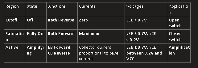
Cutoff:
BJT is off
Both junctions reverse biased
No current flow
Saturation
BJT fully on
Both junctions forward biased
Max current flow
Forward Active
BJT amplifying
EB junction forward-biased
CB junction reverse biased
Current Amplification
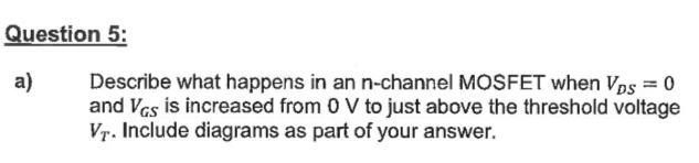
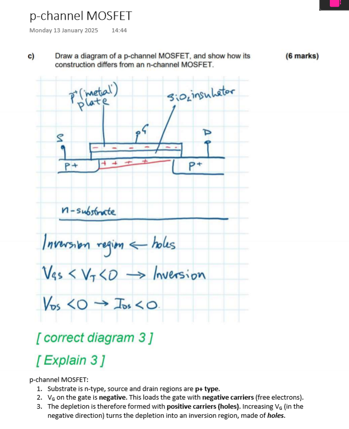
When VDS = 0 and VGS is increased from 0V to just above VT (threshold voltage)
A positive charge accumulates on the gate
Positive gate charge attracts Negative charge to the underlying p-type substrate
This attraction forms a depletion region in substrate
As VGS increases:
Negative charge @ surface of substrate increases to where p-type substrate becomes intrinsic
When VGS reaches VT:
Inversion occurs (n-type channel forms between source & drain regions)
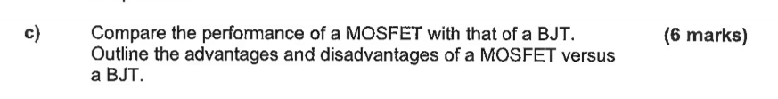
MOSFETS:
Primarily Controlled by Voltage
Easier to manage for amplification
Generally offer higher current gain
BJT:
Controlled by Current
Slightly better high-frequency performance