Looks like no one added any tags here yet for you.
What is a two port network?
A two-port network is an electrical network with two separate ports for input and output signals.
What is a port?
A port is a pair of terminals through which a signal (current) may enter or leave an electric network.
What is a newtwork?
The network consists of an interconnection of linear elements (and may include dependent sources). This could represent for example a filter or an amplifier circuit.
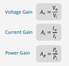
How do you calculate voltage, current and power gain?
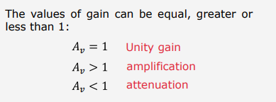
What does it mean if values of gain ae less than, equal to or greater than 1?
What is a decibel?
a unit of measuring large gain, its a unit (a logarithmic expression)
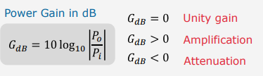
What is happening if the power gain is greater than 1?
The circuit is delivering more power to the load than it is accepting at its input. (NOTE: The power gain of modern electronic circuits is very high, typically in the magnitudes of 10^6.)
how do you calculate power gain in decibels? And what does this mean in relation to being less than, equal to or greater than zero.
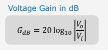
How do you calculate voltage gain in decibels?
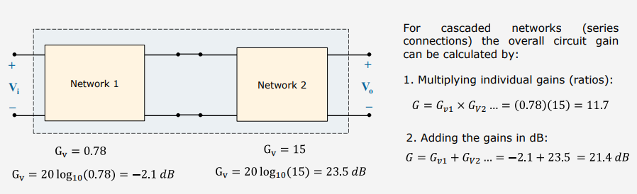
How do you calculate the overall circuit gain in a cascaded network?
Multiplying individual gains (ratios)
Adding the gains in decibels
What is frequency response?
The frequency response of the circuit refers to the way in which the gain of the circuit (magnitude and phase) changes with frequency.
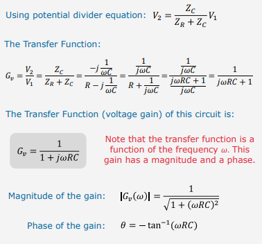
What is transfer function?
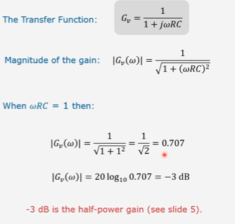
The transfer function is the ratio between the output and input signal of a two-port network - it’s an expression for the voltage gain ratio of the circuit
To analyse the frequency response of first order circuits (simple RC and RL circuits), we will use their transfer functions.
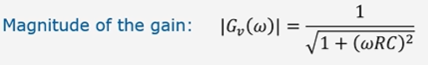
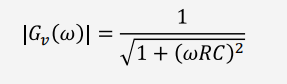
How do you calculate the magnitude of the gain?
How do you calculate the phase of the gain
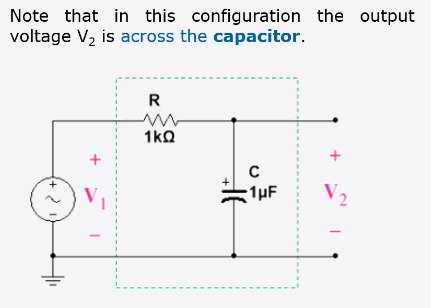
How do you derive and hence calculate the transfer function for this particular circuit
Looking at the magnitude of gain equation, what happens at low frequencies (tending to zero)?
𝜔 is small and thus the value of wRC becomes insignificant compared to 1, so that the gain tends to 1 (0 dB)
Looking at the magnitude of gain equation, what happens at high frequencies (tending to infinity) for Low filter circuits?
𝜔 is large and thus the value of becomes more significant compared to 1, so that the gain tends to 1/𝜔𝑅𝐶 meaning that the gain of the network decreases with frequency
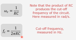
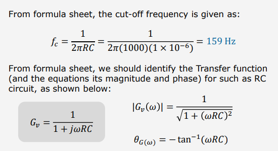
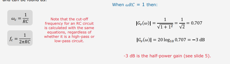
What is the cut off frequency? And how do you calculate it?
The frequency at which this half-power gain occurs
What happens if wRC is equal to 1?
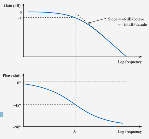
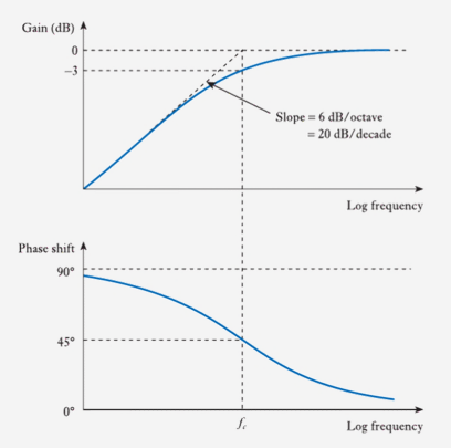
What a bode diagram?
Bode diagrams (or Bode plots) are used to graphically describe the logarithmic gain (in dB) and the phase of the circuit against logarithmic frequency
What can we see from this Bode plot (magnitude) of a low filter circuit?
Low frequency signals ( 0 < 𝑓 < 𝑓𝑐) are passed without or with very low attenuation (passband).
High frequency signals ( 𝑓 > 𝑓𝑐) are cut or attenuated (stopband).
Therefore, this circuit had the characteristics of a Low-pass filter, since is allows low-frequency signals to pass but filters out high-frequency signals.
What are the axis on a bode diagram?
log frequency (x axis) against gain (dB) or phase shift (degrees)
on the formula sheet, what is the cut of frequency and hence what are the equations you can derive from this (transfer function, magnitude, phase) for an RC circuit?
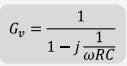
For a high pass RC circuit (where output voltage is across the resistor), how do you calculate the transfer function (voltage gain)?
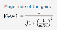
For a high pass RC circuit (where output voltage is across the resistor), how do you calculate the magnitude of gain?
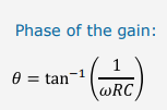
For a high pass RC circuit (where output voltage is across the resistor), how do you calculate the phase of gain?
Looking at the magnitude of gain equation for high pass circuits what happens at high frequencies (tending to infinity)?
At high frequencies (tending to infinity): 𝜔 is large and thus the magnitude of 1/𝜔𝑅𝐶 is small compared to 1, so that the value of the denominator is close to 1, and thus the gain tends to 1
Looking at the magnitude of gain equation for high pass circuits what happens at high frequencies (tending to zero)?
At low frequencies (tending to zero): The magnitude of 1 𝜔𝑅𝐶 becomes more significant and the gain decreases.
What is the cut off frequency for a high pass RC circuit?
What can we see from a bode diagram for a high pass RC circuit?
Low frequency signals ( 0 < 𝑓 < 𝑓𝑐 ) are cut or attenuated at a slope of 20 dB per decade (stopband).
High frequency signals (𝑓 > 𝑓𝑐) are passed without or with very low attenuation (passband).
Therefore, this circuit had the characteristics of a High-pass filter, since is allows high-frequency signals to pass but filters out low-frequency signals
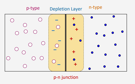
Describe the p-n junction
the p-type has many silicon atoms with a few boron where as n type has many silicon but a few phosphorous
What is the depletion layer?
The majority charge carriers on each side diffuse across the junction where they recombine with (and remove) the charge carriers of the opposite polarity.
Diffusion and recombination of charge carriers produces a region that has very few free charge carriers. This region is the depletion layer.
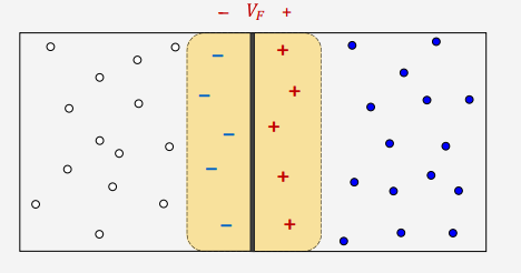
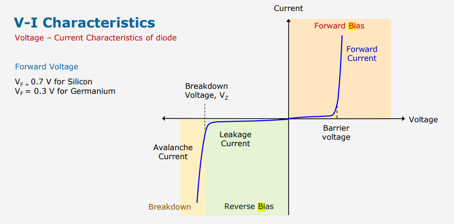
What is the barrier voltage?
The presence of negatively and positively charged ions in the depletion layer produces an electric potential across the junction: The junction potential , barrier voltage or forward voltage.
The forward voltage, V(f) is 0.7 V for silicon diodes and 0.3 V for germanium diodes.
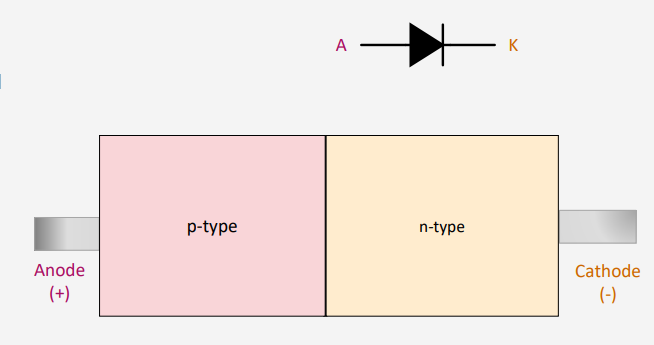
What is a diode?
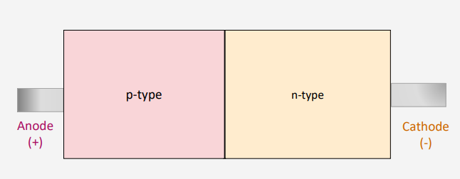
A diode is made of a semiconductor material, typically silicon, with both p-type and n-type regions forming a p-n junction.
where does the anode and cathode lie on a diode?
The Anode (+) on the p-type region side. The Cathode (-) on the n-type region side.
What is forward bias?
A positive voltage is applied across the diode (anode relative to cathode).
The bias voltage should be larger than the barrier voltage to allow movement of the majority charge carriers. (In forward bias, the diode conducts, i.e. current flows through the diode from anode to cathode only.)
What is reverse bias?
A negative voltage is applied across the diode (anode relative to cathode).
Only a very small current (negligible) flows through the diode from cathode to anode due to the movement of minority charge carriers: the leakage current. (In reverse bias, no current flows through the diode.)
Draw and label the characteristics of a diode on a V-I graph.
Include Forward Current, forward bias region, barrier voltage, leakage current, breakdown voltage, avalanche current, reverse bias region and breakdown.
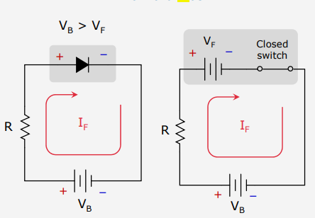
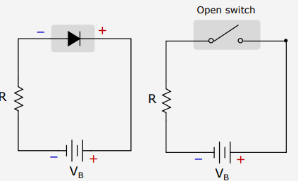
How could you represent forward bias in terms of switches?
A diode in forward bias can be represented as a closed switch in series with a voltage source (V equal to V(F) )
How could you represent reverse bias in terms of switches?
A diode in reverse bias can be represented as an open switch.
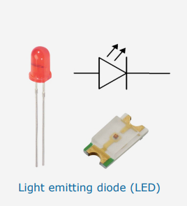
what is the symbol for a LED?
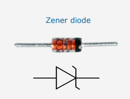
what is the symbol for a zener diode?
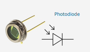
what is the symbol for a photodiode?
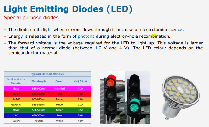
What is an LED and what are its features?
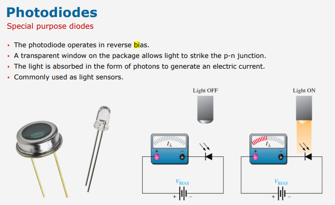
What is a photodiode and what are its features?
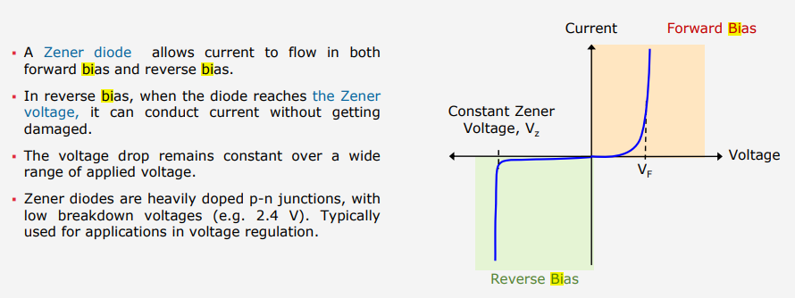
What is a Zener diode and what are its features?
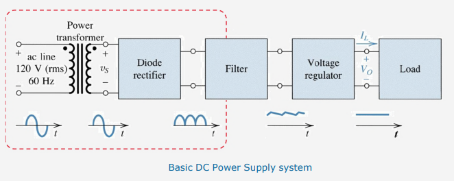
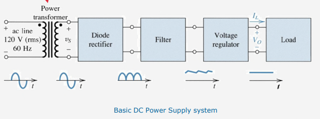
What is rectification? (DC power supply system)
Rectification is the conversion of AC voltage to DC voltage. Half-wave rectifier and Full Wave rectifier circuits are used.
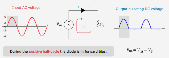
What is a half-wave rectifier? (diode rectifier circuits)
Half wave rectifiers convert an AC signal into a pulsating DC signal.
Only the positive half cycle of the input AC wave is allowed. The negative half cycle is blocked.
There is a voltage drop across the diode, V(F)
NOTE: during the negative half-cycle the diode is in reverse bias. V(RL) = 0V
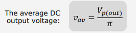
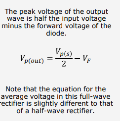
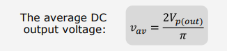
What is the average DC output voltage equation for half-wave rectifiers?
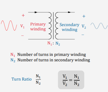
What is a transformer?
A transformer is used to transfer electrical energy between two (or more) circuits through electromagnetic induction. They are used to increase or decrease AC voltages in electric power applications.
What is the transformer equation?
what kind of wave rectifier are transformers used for?
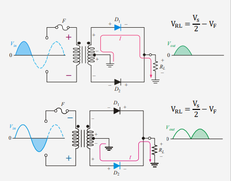
{Note that the output voltage is halved when measuring with reference to the centre tap.}
This transformer is used for the “Centre-tapped full wave rectifier circuit” configuration.
what transformer is used in a centre-tapped full wave rectifier?
In a centre-tapped full-wave rectifier circuit, a center-tapped transformer is used with two diodes. Each diode conducts on alternating half-cycles.
During the positive half cycle, the D1 is forward-biased and the D2 is reverse biased.
During the negative half cycle, D1 is forward-biased and D2 is reverse-biased.
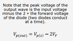
How do you calculate the peak voltage of the output wave from a centre-tapered full wave rectifier?
How do you calculate the average DC output voltage of a centre-tapered full wave rectifier and a bridge full-wave recifier?
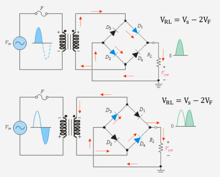
What is a bridge full wave rectifier?
The bridge full-wave rectifier circuit uses four diodes connected in bridge configuration across the entire secondary winding of a simple transformer.
During the positive half cycle, D1 and D2 conduct in series, while D3 and D4 are reverse-biased.
During the negative half cycle, D3 and D4 conduct in series, while D1 and D2 are reverse- biased.
How do you calculate the peak voltage of the output wave
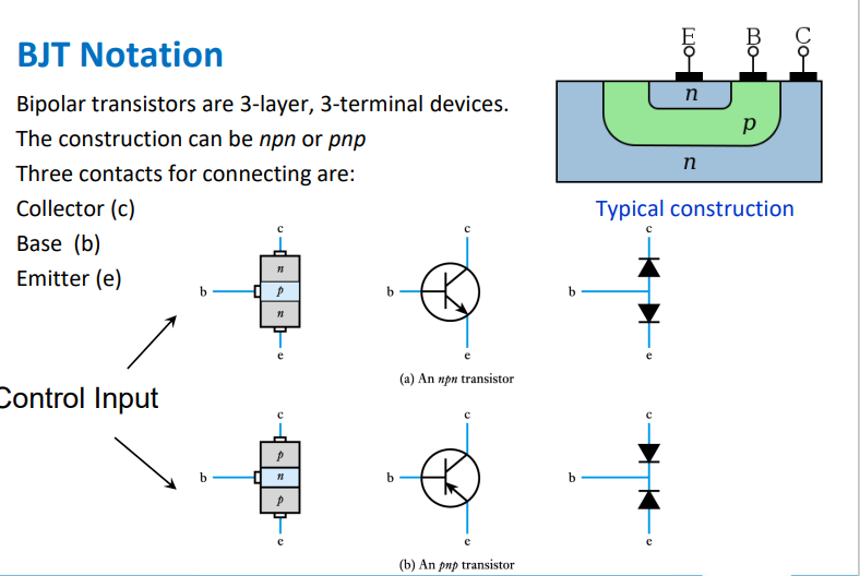
What is a bipolar junction transistor?
A bipolar junction transistor is constructed with three doped semiconductor regions separated by two pn junctions.
It has three terminals: Emitter (E), Base (B), and Collector (C).
An npn transistor (95%+ of usage) has a p region between the two n regions. A pnp transistor (<5% usage) has an n region between the two p regions.
What is the BJT notation?
Bipolar transistors are 3-layer, 3-terminal devices. The construction can be npn or pnp
Three contacts for connecting are: Collector (c) Base (b) Emitter (e)
How does a BJT operate?
Flow of charges (current) in a BJT occurs due to diffusion of charges across a PN junction of two regions with different charge concentrations.
The emitter region is heavily doped, compared to the other two layers.
The base is very narrow (tens on microns).
When sufficient (above 0.7 V) VBE is applied (forward bias), it starts a flow of electrons from a high-concentration emitter into the base (base current flows in).
Electrons are minority carriers in the p base, so a vast majority of them diffuses towards the collector. i.e. only a fraction (1% or so) of electrons actually flows through the base.
This amplification effect is approx. 100 to 300 in the linear region. ▪ Hence controlling the small IB controls the larger currents IC , I E
BJT needs to be properly polarised, see below.
Small base-to-emitter current causes much larger collector-to-emitter current (“ON” condition).
Removal of the base current stops the flow of electrons and holes - effectively turns the transistor OFF.
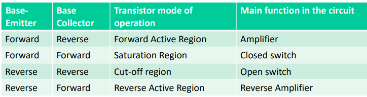
What are the modes of operation?
The DC voltage sources connected to the transistor determine the mode of operation of the transistor.
Depending on the biasing of the two diodes, there are four modes of operations for a transistor
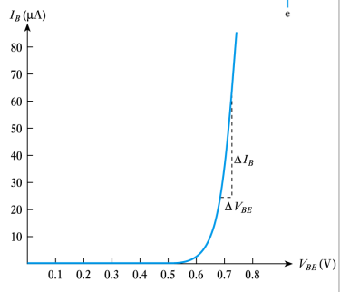
What are the input characteristics of a bipolar transistor?
The input is actually a forward-biased pn junction.
The input characteristics is the same as in a diode.
Very little base current until V(BE) reaches 0.6 or 0.7 V, then it passes a lot of base current.
A resistor in series will prevent excessive base current.
NOTE: Base-emitter junction behaves like a normal diode. In both Active and Saturation it is Forward Biased, with approx. 0.7 V across it.
What are the input characteristics of a bipolar transistor?
The collector current mostly depends on the base current.
This is not true in the region near the origin (low VCE), the saturation region.
Saturation region is used when BJT should act as a switch. Normally it is avoided in linear circuits.
To act as a good amplifier of small signals, BJT needs to work in the middle of the active region.
In the active region the value of 𝐼𝐶 is almost constant and given by 𝐼𝐶 = ℎ(fe) I(B)
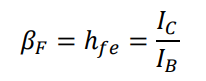
What is the current gain of a transistor? How do you calculate it?
Low-power transistors have a large gain when in the active region (proper polarization), typically from 100 to 300. his large ratio between IC and IB makes the bipolar NPN transistor a very useful amplifying device.
Also, as the power rating goes up, transistors get larger, the current gain becomes smaller, dropping to 20 or less.
This relationship holds only in the active region (not in saturation nor in cut-off regions).
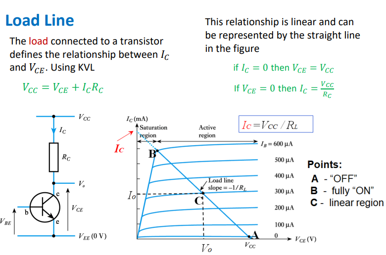
What is the load line?
What is BJT Saturation?
This happens when BOTH PN junctions are FB and the collector current becomes so large that C-E voltage falls below 0.2 or 0.3 V. The reasons can be:
• base current is too large,
• RC is too large,
• VCC is insufficient for the collector-emitter circuit.
This is a good operating regime if we want the BJT to operate as a switch – fully switched ON and the C-E current mostly depends on the outside components
What is BJT Cut-Off?
This happens when BOTH PN junctions are RB.
The base and collector currents are very low (≈zero). VCE=VCC
This is a good operating regime if we want the BJT to operate as a switch – Open Switch.
slide 14 - 23
What is an operational amplifier?
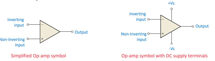
An operational amplifier, or op-amp is an active device designed to perform mathematical operations, such addition, subtraction, integration and differentiation; hence the term operational. As an active element, the op-amp must be powered by a voltage supply. For simplicity, the power supply terminals are often ignored in circuit diagrams.
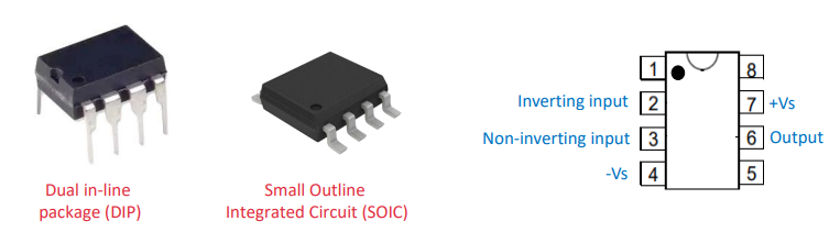
***(The op-amp is a versatile building block, and thus is among the most widely used electronic devices. Op-amps are commercially available in integrated circuit (IC) packages such as dual-in-line package (DIP) or small outline integrated circuit (SOIC))***
what does the voltage amplifier and an output amplifier do in a operational amplifier?
The voltage amplifier provides high voltage gain.
The output amplifier provides high current gain.
What are the typical characteristics of a non-ideal op-amp?
Very high open loop gain (in the order of 105 )
The differential input is very small, Vin < 100 µV
The input resistance is around 10 MΩ
The input current is a few nA
Output resistance is small, between 10 and 100 Ω
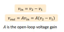
What is the main equations to find v out and v in for an op-amp?
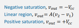
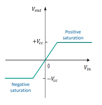
What output voltage can a op-amp not exceed?
+V(cc) or -V(cc)
What three regions can an op-amp operate in?
what happens if you increase the differential input beyond the linear region?
The op-amp will be saturated
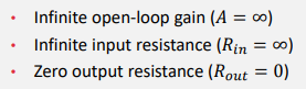
What are the characteristics for an ideal op-amp?