L12 Electronic Properties of Solids
1/7
There's no tags or description
Looks like no tags are added yet.
Name | Mastery | Learn | Test | Matching | Spaced | Call with Kai |
|---|
No study sessions yet.
8 Terms
Sigma bonds vs pi bonds in a large molecule and effect on properties
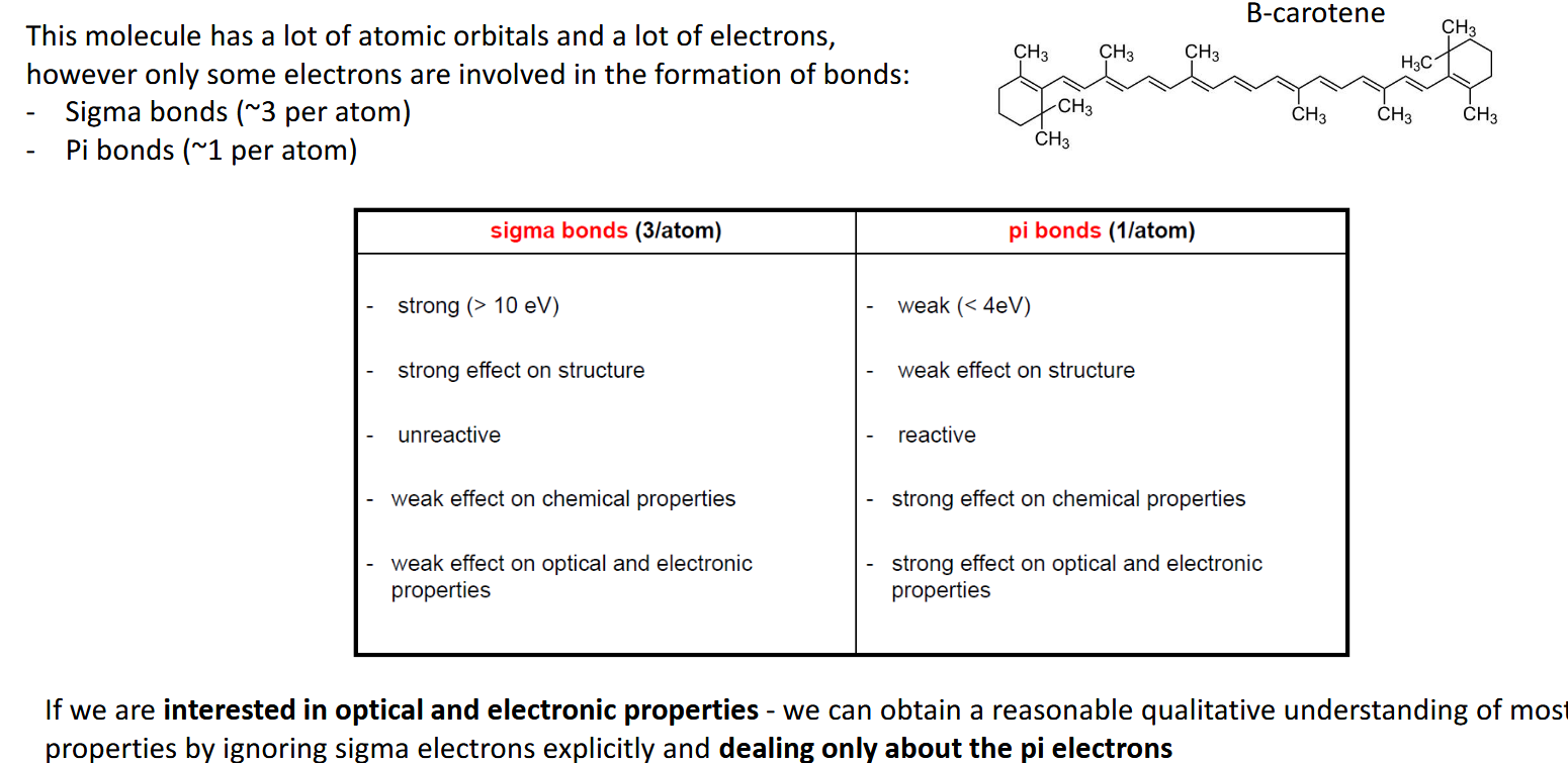
How can we approximate theinteractions in large molecules
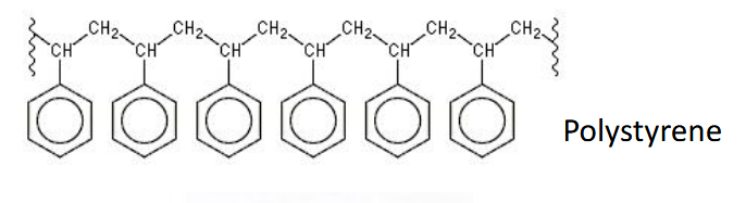
Consider only the pi electron interactions. In a large molecule without extensive conjugation, optical and electronic properties will be defined by the properties of its individual conjugated segments e.g. in polystyrene
Huckel approximation (pi electron interactions) in a large molecule
Only consider interactions with the carbons directly either side and we assume their local environment is all the same
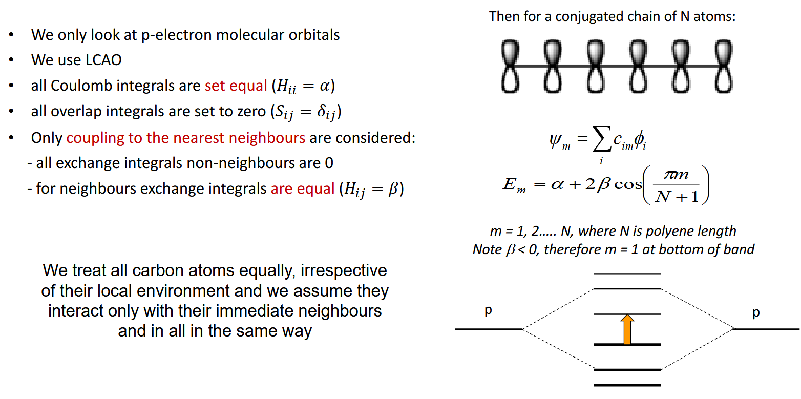
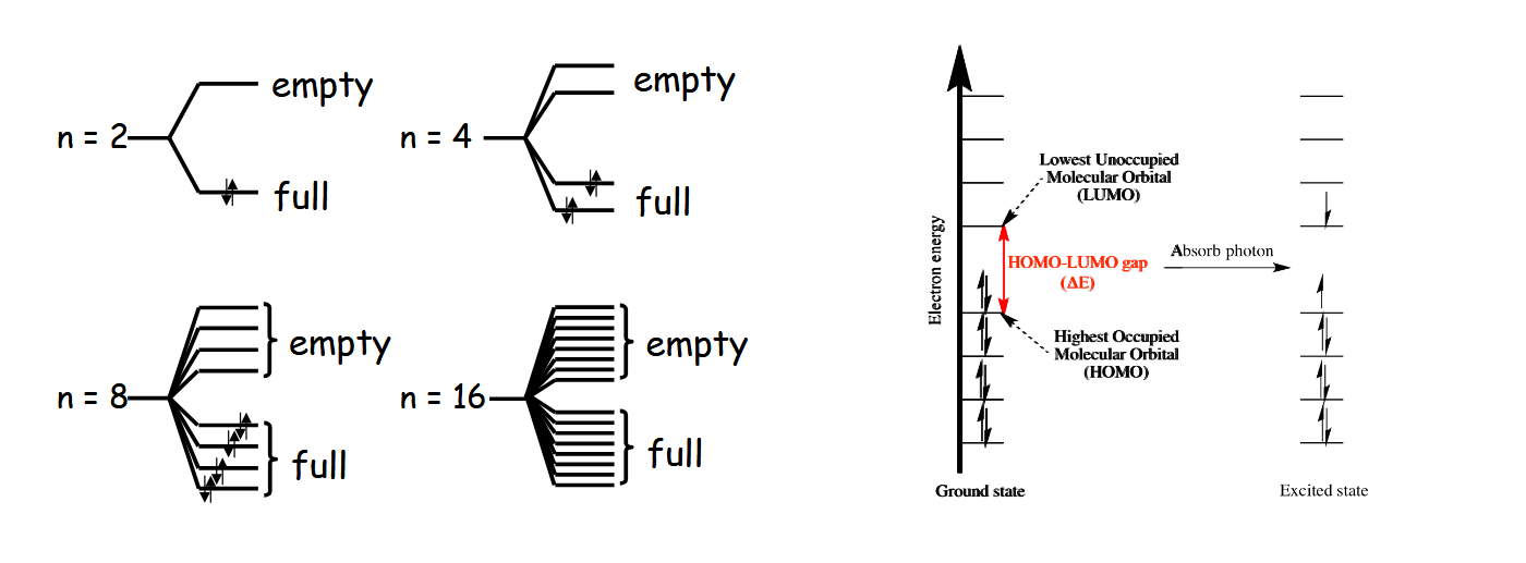
What happens as the number of carbons and pi electrons increases
An almost continuous band of energy levels forms, leaving the HOMO and LUMO clearly identifiable at the top of the valence band and bottom of the conduction band respectively. The energy gap between them is the optical gap corresponding to the energy absorbed from a photon. The optical gap shrinks as conjugation length increases
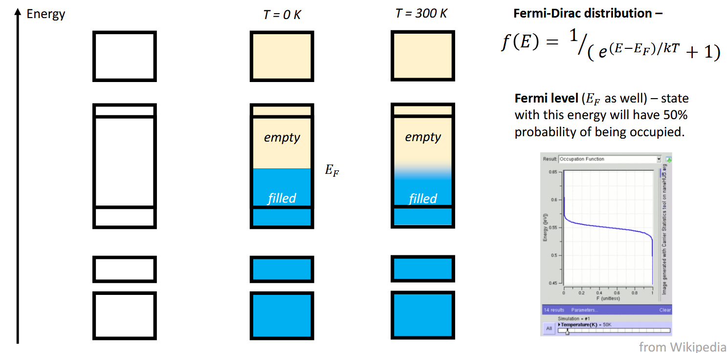
What is Fermi energy EF
States with this energy will have 50% probability of being occupied.
Note that in real systems, the line between the empty and filled states is blurred as not all electrons have the same energy (temperature). Hence the filled energy levels are not just the lowest ones.
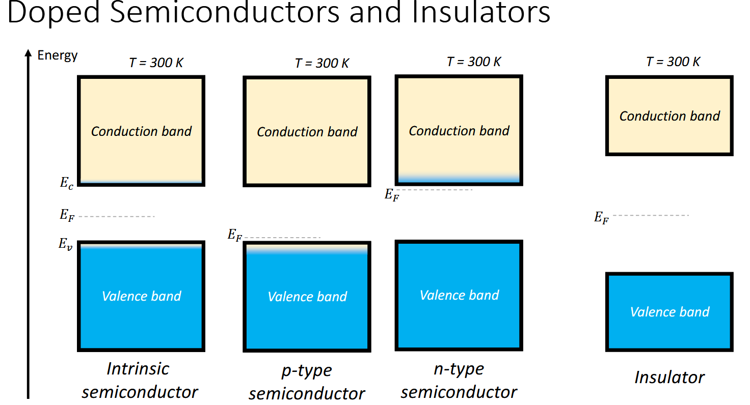
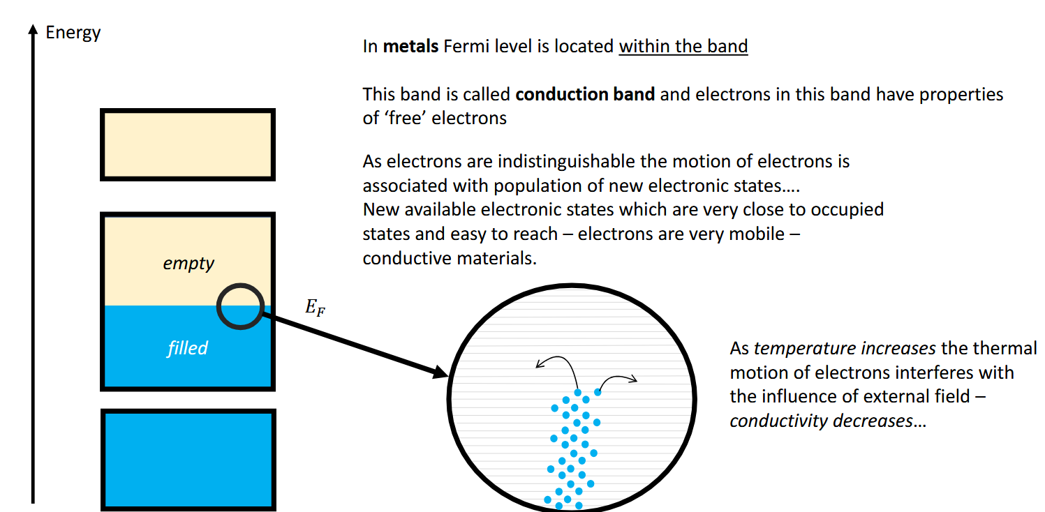
What band is the Fermi level located in metals and how does this tie in to conductivity.
The conduction band - there is no band gap.
Metals are conductive thanks to the “free” nature of the electrons in the band.
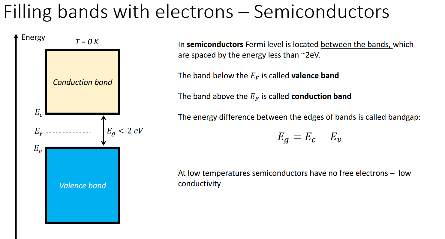
What about the Fermi level in semiconductors
What energy gap do semiconductors have in eV
The Fermi level is located within the band gap, above the valence band and below the conduction band.
The conductivty in semiconductors is dependent on being able to jump the band gap. At low temperatures, electrons cannot reside in the conduction band hence semiconductors only conduct abve a certain temperature.
Less than about 2 eV - higher and they are insulators (dielectric)
How can you alter the properties of a semiconductor and what does it do
By doping it, you can add some holes in the valence band (p-type) or add some mobile electrons (n-type)
p-type lowers the Fermi level
n-type increases the Fermi level
Wide band gaps produce insulators (dielectric)