Solid State Materials and Modelling
1/105
There's no tags or description
Looks like no tags are added yet.
Name | Mastery | Learn | Test | Matching | Spaced | Call with Kai |
|---|
No analytics yet
Send a link to your students to track their progress
106 Terms
What factors determine the physical properties of solid-state materials?
The physical properties are determined by the properties of constituent atoms, local interactions of atoms, and the three-dimensional arrangement of atoms in the solid.
What are the seven types of crystal lattices?
The seven types of crystal lattices are: cubic, tetragonal, orthorhombic, rhombohedral, hexagonal, monoclinic, and triclinic
How many total Bravais lattices are there
There are 14 Bravais lattices.
What are the two packing configurations mentioned in the lecture?
The two packing configurations are Face-Centered Cubic (FCC) ABCABC and Hexagonal Close Packing (HCP) ABABAB.
Describe the CsCl crystal structure.
In the CsCl structure, Cl− ions form a simple cubic lattice while Cs+ ions fill the octahedral holes at a position of Z=0.5
What underlies the differences between diamond and graphite structures?
Diamond has a sp3 hybridization leading to a tetrahedral arrangement, whereas graphite has sp2 hybridization resulting in planar layers.
What types of solids are classified as crystalline and amorphous?
Crystalline solids have a regular atomic arrangement with long-range order, while amorphous solids have short-range order without long-range periodicity.
What defines short-range order (SRO) and long-range order (LRO)?
SRO refers to similar arrangements of nearest neighbors among atoms, while LRO indicates a periodic arrangement extending over large distances, typical of perfect crystals
What are the main types of disorder that can affect crystalline structure
Structural disorder (displacement of atoms) and chemical disorder (occupancy of lattice sites by different atoms)
What is the significance of crystallite size in materials?
Crystallite size can classify materials into polycrystalline, microcrystalline, nanocrystalline, and amorphous categories, affecting their overall properties.
What is a perovskite structure?
A perovskite structure is represented by the formula ABX3, where a cation A forms an FCC lattice and a cation B fills some of the octahedral holes.
Spinel structures, normal vs inverse
In normal spinel, cations occupy (A, 1/8) tetrahedral and (B, 1/2) octahedral holes; in inverse spinel, A, ¼ oct., B ¼ oct., B 1/8 tet.
What is the equilibrium constant for Schottky defects?
( K_{Schottky} = \frac{[Na^+]^2 \cdot [V^{•}] \cdot [Cl^-]^2}{[NaCl(s)]} )
How is the number of Schottky defects represented?
( ns = N \cdot K{Schottky} ) or other eq.
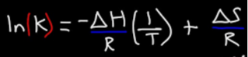
What is the equation that relates equilibrium constant to enthalpy and entropy?
( \ln K_{eq} = -\frac{ΔH}{RT} + \frac{ΔS}{R} )
What is the expression for the number of Frenkel defects?
( n_F = N \cdot N_i \cdot \frac{1}{2} \exp\left(-\frac{ΔH_F}{2kT}\right) )
What does the formulation ( ΔG = ΔH - TΔS ) represent in terms of defect formation?
This equation represents the free energy change associated with defect formation.
How is the change in entropy for defect formation calculated?
( ΔS = k \ln W ), where (W) is the number of ways to distribute defects.
What are intrinsic defects?
Defects that arise naturally due to thermodynamic reasons, including vacancies and interstitials.
What constitutes extrinsic defects?
Defects that are introduced intentionally through processes like doping or purification.
What is the difference between point defects and extended defects?
Point defects occur at single sites (like vacancies), while extended defects span one, two, or three dimensions (like dislocations and grain boundaries).
What are Schottky defects?
A type of defect involving pairs of vacancies that maintain charge neutrality in ionic crystals.
What are Frenkel defects?
Defects that consist of a vacancy and an interstitial, affecting charge distribution.
How do dislocations affect material properties?
Dislocations enable plastic deformation and are critical in determining the strength and ductility of materials.
What do grain boundaries represent in crystalline materials?
Interfaces between different crystallites that affect dislocation movement and mechanical properties.
What are twins in crystal structures?
Boundaries where part of the crystal lattice mirrors the structure on the opposite side, influencing various material properties.
What is the band structure in solid-state physics?
A band structure is a plot of electron energy (E) versus wave vector (k) that describes the energy levels of electrons in a solid.
How does the band structure differentiate metals, semiconductors, and insulators?
In metals, the Fermi level cuts through a band; in semiconductors, there is a gap between filled and unoccupied states; in insulators, this gap is larger.
What does the Density of States (DOS) represent?
The DOS indicates the number of electronic states at a specific energy level available for occupancy in a material.
What materials properties are linked to band structure?
Band structure is linked to electronic conductivity, optical properties, structural distortions, mechanical properties, and catalytic activity.
How does orbital overlap affect band structure?
Increased orbital overlap leads to wider bands that correspond to delocalized electrons, impacting bonding and material properties.
Why is understanding the electronic structure critical?
It informs the relationship between a material’s structure and its properties, enabling applications in solid-state physics and materials engineering.
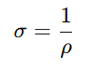
What is the difference between resistivity and conductivity?
Resistivity (ρ) measures how strongly a material opposes current flow, while conductivity (σ) is its inverse, indicating how well the material conducts electricity.
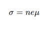
What is the relationship between resistivity (ρ) and conductivity (σ)?
σ = 1/ρ.
Why do metals have high conductivity?
The Fermi level cuts through a partially filled band, allowing free electron movement.
What makes a material a semiconductor?
A band gap exists between the conduction and valence bands, limiting electron movement at low temperatures.
What factors affect carrier mobility (μ)?
Carrier concentration (n), effective mass (m*), and relaxation time (τ).
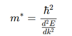
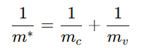
How does effective mass affect conductivity (+ equation)?
A smaller effective mass results in higher mobility and better conductivity.

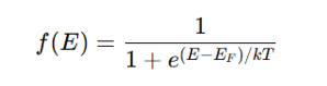
What is the significance of the Fermi level (EF) for the Fermi Dirac distribution?
It is the energy level where the probability of electron occupation is 50%.
How does temperature affect the Fermi-Dirac distribution?
Higher temperatures increase electron excitation, shifting distribution slightly.
How does temperature affect metal conductivity?
Conductivity decreases with temperature due to increased scattering by phonons.
How does temperature affect semiconductor conductivity?
Conductivity increases as more electrons are thermally excited across the band gap.
What is the difference between a direct and indirect band gap?
Direct band gaps allow electron transitions without phonons, while indirect band gaps require phonons, making transitions less efficient and or crystal momentum of electrons and holes is the same in both the conduction band and the valence band.
Give an example of a direct band gap semiconductor.
Gallium Arsenide (GaAs).
Give an example of an indirect band gap semiconductor.
Silicon (Si)
Why is high mobility important in semiconductors?
It improves performance in devices like transistors and solar cells.
What are some common semiconductor structures?
Diamond (Si, Ge), Sphalerite (GaAs, ZnS), and Chalcopyrite (CuFeS2).
What is the relationship between resistivity (ρ) and conductivity (σ)?
σ (Conductivity): Measures how well a material conducts electricity (S/cm).
ρ (Resistivity): Measures how strongly a material opposes current flow (Ω·cm).
Low resistivity → High conductivity.
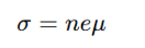
What equation relates conductivity (σ) to microscopic electron properties?
where:
n = Carrier concentration (cm−3^{-3}−3)
e = Elementary charge (1.602×10−191.602 \times 10^{-19}1.602×10⁻¹⁹ C)
μ = Carrier mobility (cm2^22/V·s)
σ increases if there are more free charge carriers or if they move faster.
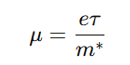
How is carrier mobility (μ) defined?
where:
e = Elementary charge
τ = Relaxation time (time between collisions)
m∗ = Effective mass of charge carrier
Higher μ means less scattering, leading to better conductivity.
How does effective mass (m*) relate to the band structure?
where:
E(k) = Energy dispersion relation (band structure)
ℏ = Reduced Planck’s constant (h2π\frac{h}{2\pi}2πh)
k = Wavevector (momentum representation in crystals)
Smaller m∗ → Faster electrons → Higher conductivity.
What is the Fermi-Dirac distribution equation?
where:
f(E) = Probability of an energy state EEE being occupied by an electron
E_F = Fermi energy
k = Boltzmann constant
T = Temperature
Higher T → More electrons excited to conduction band.
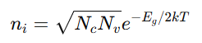
What equation describes the intrinsic carrier concentration?
where:
N_i = Intrinsic carrier concentration
E_g = Band gap energy
N_c, N_v = Effective density of states in conduction/valence bands
As T increases, n_i increases exponentially.
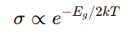
Temperature dependence of conductivity in semiconductors, equation
What is the difference between intrinsic and extrinsic semiconductors?
Intrinsic semiconductors have a low charge carrier concentration, while extrinsic semiconductors are doped to increase conductivity.
How does doping affect a semiconductor?
It introduces additional charge carriers (electrons or holes), modifying electrical properties.
What type of charge carriers does n-type doping introduce?
Electrons
What type of charge carriers does p-type doping introduce?
Holes
How does n-type doping affect the Fermi level?
It raises the Fermi level closer to the conduction band.
How does p-type doping affect the Fermi level?
It lowers the Fermi level closer to the valence band.
What happens at a p-n junction?
Electrons diffuse from n-type to p-type, and holes diffuse in the opposite direction, creating a depletion region.
What is the depletion region?
A region near the p-n junction depleted of free charge carriers, acting as an insulator.
What is forward bias in a p-n junction?
An external voltage reduces the depletion region, allowing current flow.
What is reverse bias in a p-n junction?
An external voltage expands the depletion region, preventing current flow.
What is the photovoltaic effect?
The generation of voltage or current in a material upon light exposure.
How do LEDs produce light?
Electrons recombine with holes, releasing energy as photons.
Name three devices that use p-n junctions.
Solar cells, LEDs, transistors.
How does an OLED differ from an LED?
OLEDs use organic materials and multi-layer structures for efficient light emission.
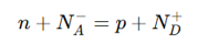
Charge neutrality condition (in doped semiconductors)
where:
N_A^- = Ionized acceptor concentration (p-type)
N_D^+ = Ionized donor concentration (n-type)
Ensures total charge balance.
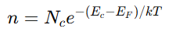
carrier concentration in n-type semiconductors
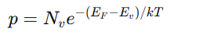
carrier concentration in p-type semiconductors
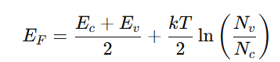
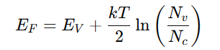
position of the fermi level in an intrinsic semiconductor
where:
E_F = Fermi energy
E_c, E_v = Conduction and valence band energies
N_v, N_c = Density of states
For intrinsic semiconductors, E_F lies close to the middle of the band gap.
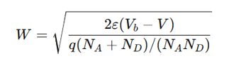
depletion region width in a p-n junction
where:
ε = Permittivity of semiconductor
V_b = Built-in voltage
V = Applied voltage
N_A, N_D = Acceptor/donor concentrations
Larger V_b → Wider depletion region.
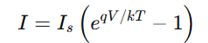
Current flow in a forward-biased p-n junction, equation
where:
I_s = Reverse saturation current
q = Electron charge
V = Applied voltage
Current increases exponentially with V.
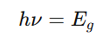
Photovoltaic Effect (Solar Cells), when is photon energy sufficient
where:
hν = Photon energy
E_g = Band gap energy
Light with energy ≥ E_g excites electrons to conduction band.

what causes light emission in LEDs
Electron-hole recombination emits a photon with energy equal to the band gap.
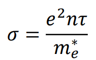
how does conductivity, relaxation time equation
n carrier concentration, is constant in metals (many free electrons).
τ = the relaxation time (s) {the time between collisions}
How does semiconductor conductivity depend on temperature (+ equation)
σ∝e−Eg/2kT\sigma \propto e^{-E_g / 2kT}σ∝e−Eg/2kT
As T increases, more electrons are excited across the band gap.
Large E_g → Lower conductivity at room temperature (e.g., insulators).
Small E_g → More thermally excited carriers (e.g., semiconductors).
What defines a transparent conducting oxide (TCO)?
A material that is electrically conductive while remaining optically transparent
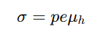
How is conductivity (σ) related to charge carriers?
where:
n = Carrier concentration (cm−3^{-3}−3)
e = Electron charge (1.602×10−191.602 \times 10^{-19}1.602×10⁻¹⁹ C)
μ = Carrier mobility (cm2^22/V·s)
Higher n or μ improves conductivity.
2 methods of TCO doping?
n-type TCOs (donor doping): Electrons from oxygen vacancies or metal interstitials.
p-type TCOs (acceptor doping): Holes from cation vacancies or oxygen interstitials.
How are charge carriers generated in n-type TCOs? chem eq
VO⋅⋅ = Oxygen vacancy
O_O = Oxygen atom in the lattice
Generates free electrons, increasing conductivity.
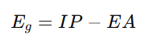
What is the difference between the fundamental and optical band gaps?
o IP = Ionization potential
o EA = Electron affinity
Optical band gap:
o Determined by allowed optical transitions.
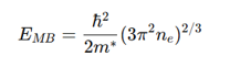
Moss-Burstein shift
where:
E_{MB} = Energy shift
m^* = Effective mass of electrons
n_e = Electron concentration
Higher n_e increases optical band gap.
Effective mass of charge carriers
What makes Indium Tin Oxide (ITO) the most widely used TCO?
Low resistivity (~10−4Ω10^{-4} \Omega10−4Ωcm).
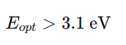
Optical band gap of 3.7 eV (high transparency).
Easy to etch (for manufacturing).
Why is ZnO a promising TCO alternative?
Earth-abundant and non-toxic.
Direct band gap (3.37 eV).
Can be doped with Al, Ga, In for high conductivity.
Why are p-type TCOs difficult to fabricate?
Oxygen 2p valence bands lie too deep → High ionization potential.
p-type defects are often compensated by electrons → Low carrier concentration.
What strategies help create p-type TCOs?
Valence Band Modulation: Mix Cu 3d and O 2p orbitals (e.g., Cu₂O).
Use layered oxychalcogenides: Improve valence band dispersion (e.g., LaCuOSe).
What are some of the most promising p-type TCOs?
Cu₂O: Good hole mobility but not transparent.
CuAlO₂: First transparent p-type oxide (low conductivity).
LaCuOSe: Best p-type TCO (high mobility, used in OLEDs).
Transparency condition for n-type TCOs
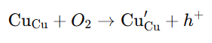
p-type conductivity in Cu2O (how they form eq.)
strategies for p-type TCOs (valence band modulation)
Valence Band Modulation: Mix Cu 3d and O 2p orbitals (e.g., Cu₂O).
Use layered oxychalcogenides: Improve valence band dispersion (e.g., LaCuOSe).
conductivity of p-type LaCuOSe, eq.
What is Hybrid DFT, and why is it used in semiconductor modeling?
Hybrid DFT mixes a percentage of Hartree-Fock (HF) exchange with DFT exchange and correlation to improve the accuracy of band gap predictions in semiconductors. It is used because standard DFT often underestimates band gaps.
How does Hybrid DFT improve band gap predictions?
Hybrid DFT methods like HSE06 and PBE0 provide more accurate band gap predictions by incorporating a portion of HF exchange. HSE06 is better for smaller band gaps, while PBE0 is better for larger band gaps.
What are charged defects, and why are they important in semiconductors?
Charged defects are imperfections in a semiconductor lattice that carry a net charge. They are important because they influence the electrical properties of the material, such as conductivity and carrier concentration.
What is the Fermi energy, and how does it affect defect formation energies?
The Fermi energy (E_F) is the energy required to add or remove an electron from the system. Defect formation energies depend on E_F, with positive defects becoming less stable as E_F increases, and negative defects becoming more stable.
What are transition levels in defect calculations?
Transition levels are the Fermi energies at which the formation energies of different charge states of a defect are equal. They indicate the ionization levels of defects and help determine the most stable charge state at a given Fermi energy.
Why are supercells used in defect calculations?
Supercells are used to model defects at infinite dilution, preventing interactions between periodic images of defects. This allows for accurate calculation of defect formation energies in a periodic system.