4.1.2 TRANSISTORS 3 QUESTIONS (LEVEL 1)
1/15
There's no tags or description
Looks like no tags are added yet.
Name | Mastery | Learn | Test | Matching | Spaced | Call with Kai |
|---|
No analytics yet
Send a link to your students to track their progress
16 Terms
Bipolar Junction Transistor (BJT)
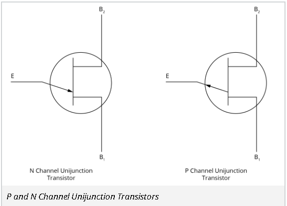
Uni-junction Transistor
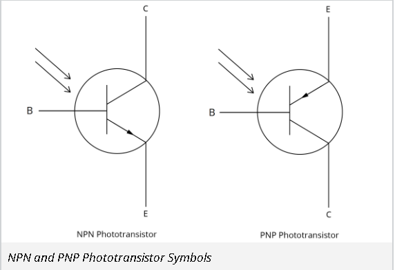
Phototransistor
NOTE THE PNP AND NPN CONFIGURATION OF ARROWS
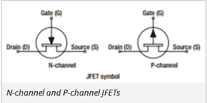
Junction Field Effect Transistor (JFET)
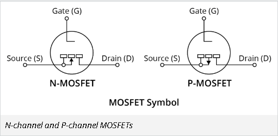
Metal Oxide Semiconductor Field Effect Transistor (MOSFET)
MTERIALS USED FOR TRANSISTORS (SEMI - CONDUCTORS)
silicon
germanium
gallium-arsenide.
PHOTODIODES NOTE
can be either BJTs or FETs.
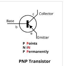
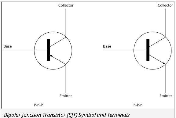
PNP (THEY WILL GIVE “BASE” SO ORIENTATION DOESNT MATTER LEARN POSITION OF “EMITTER”)
BJT PNP
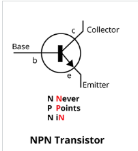
NPN (THEY WILL GIVE “BASE” SO ORIENTATION DOESNT MATTER LEARN POSITION OF “EMITTER”)
BJT NPN
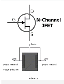
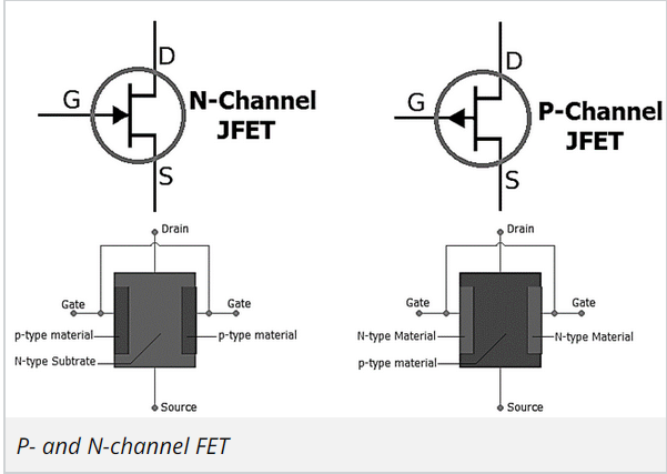
N CHANNEL (JFET)
The Field effect devices are those in which current is controlled by the action of an electron field, rather than carrier injection. Field-effect transistors are so named because a weak electrical signal coming in through one electrode creates an electrical field through the rest of the transistor.
The FET was known as a 'unipolar' transistor.
The term refers to the fact that current is transported by carriers of one polarity (majority), whereas in the conventional bipolar transistor carriers of both polarities (majority and minority) are involved.
In the BJT current (in mA) is used to control the flow of electrons between the emitter and the collector. In a FET, an electrical field, (voltage rather than current) is used to control the flow of electrons between the Source and the Drain.
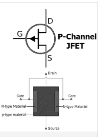
P CHANNEL (JFET)
The Field effect devices are those in which current is controlled by the action of an electron field, rather than carrier injection. Field-effect transistors are so named because a weak electrical signal coming in through one electrode creates an electrical field through the rest of the transistor.
The FET was known as a 'unipolar' transistor.
The term refers to the fact that current is transported by carriers of one polarity (majority), whereas in the conventional bipolar transistor carriers of both polarities (majority and minority) are involved.
In the BJT current (in mA) is used to control the flow of electrons between the emitter and the collector. In a FET, an electrical field, (voltage rather than current) is used to control the flow of electrons between the Source and the Drain.
TRANSISTORS NOTE
In the BJT current (in mA) is used to control the flow of electrons between the emitter and the collector. In a FET, an electrical field, (voltage rather than current) is used to control the flow of electrons between the Source and the Drain
Basic Transistor Action
When a transistor is fully on or saturated, it acts like a switch, with a small input voltage controlling a large current.
Basic Transistor Action
If the transistor is operating in the region between cut‑off and saturation, it then acts more like an amplifier.
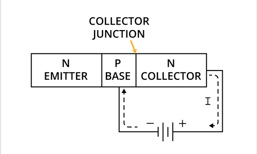
Reverse Biasing
If an external voltage is applied between the base and collector of an NPN transistor, the junction formed between the regions is called the collector-base junction or collector junction. This acts like a reverse-biased PN diode and will not conduct.
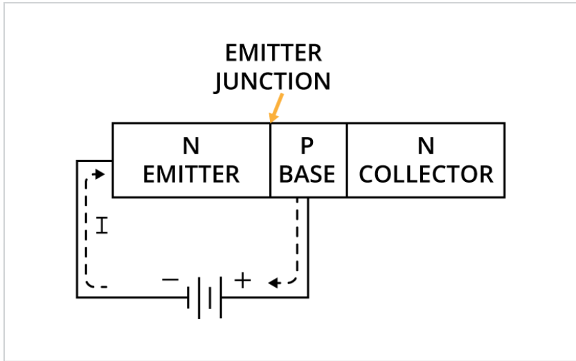
Forward Biasing
If the external voltage is now applied between the base and emitter of the transistor, the junction formed between the regions is called the emitter-base junction or emitter junction. This now acts like a forward-biased PN diode and will conduct.