FET
1/76
There's no tags or description
Looks like no tags are added yet.
Name | Mastery | Learn | Test | Matching | Spaced | Call with Kai |
|---|
No analytics yet
Send a link to your students to track their progress
77 Terms
What is a JFET?
A type of FET that operates with a reverse-biased PN junction to control current in a channel
What is JFET short for?
Junction field-effect transistor
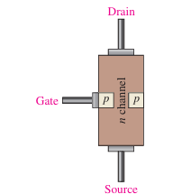
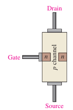
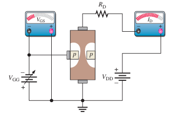
Draw a basic structure representation of n-channel of a JFET
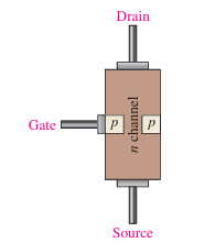
Draw a basic structure representation of p-channel of a JFET
Are the p-type regions both connected to the gate-lead?
Yes, they are connected internally. This allows to create a depletion region symmetrically from both sides in the n-channel, which allows for better control on the current
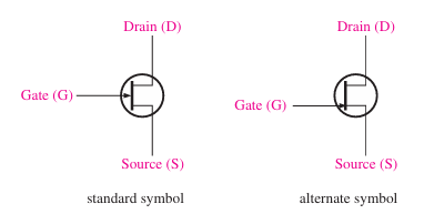
Draw the symbol for a n-channel JFET
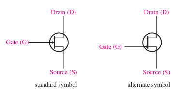
Draw the symbol for a p-channel JFET
How is the drain current controlled in a JFET
As you increase the voltage to the gate, the channel narrows (depletion region increases), which increases the resistance of the channel and decrease the drain current (Vise versa for decreasing Vgg)
Draw the drain characteristic curve for JFET (VGS = 0V)

What is the pinch-off voltage (Vp)
(For VGS = 0V) The value of VDS where ID becomes constant
What is the cutoff voltage VGS(Off)
It is where ID = 0
Explain what happens to the depletion region to allow an ohmic region to exist
The channel resistance is constant-ish because the depletion region is not large enough
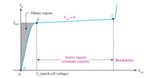
How is the drain current constant in the active region?
As VDS increases, the reverse-biased voltage VGD produces a depletion region large enough to offset the increase VDS and therefore, ID is constant
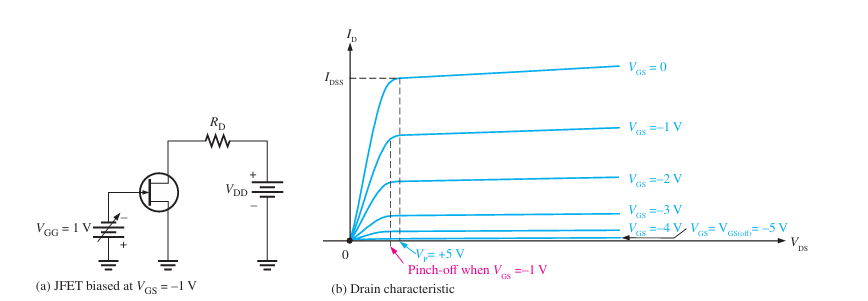
Draw a family of drain characteristics for JFET where VGS from 0V to -5V
The knee is equal to VGS - Vp and you can find the effective IDSS from the Shockley's equation
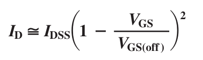
What is the Shockley's equation
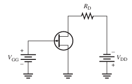
What is the difference between a p-channel JFET biasing compared to n-channel?
The polarity of the voltages
What is the relationship between VP and VGS(Off) ?
They are same in magnitude but opposite in sign
Draw the JFET universal transfer characteristics
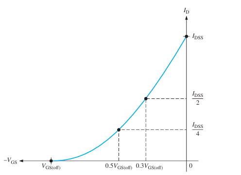
Draw the JFET universal transfer characteristics and drain characteristics curves on the same graph
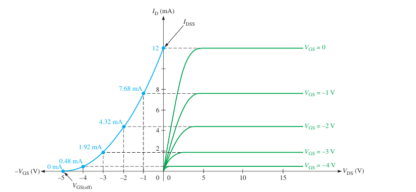
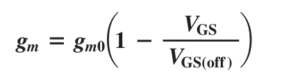
What is forward transconductance gm
It is an AC quantity that is defined as a change in drain current ΔID divided by corresponding in gate to source voltage ΔVGS with the drain-to-source voltage constant
What is the formula for forward transconductance gm
Unit: S (Siemans)
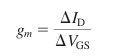
Show how you find gm from the transfer characteristic curve
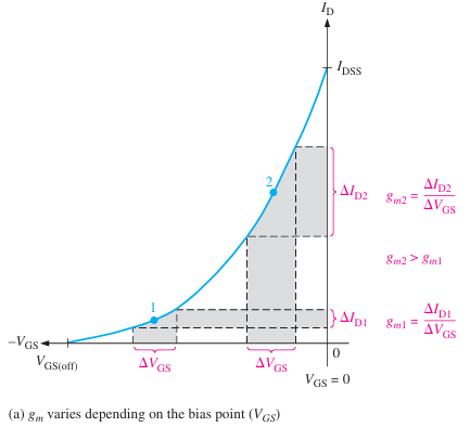
Plot gm in terms of VGS
How do you calculate gm
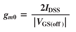
How do you calculate gm0 / gsf(max)
Note VGS =0V
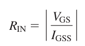
How do you calculate input resistance for a JFET?
Explain how JFET have high input resistance
JEFT operate with gate-source junction reverse-biased → high input resistance (Which means no current is drawn → no load / voltage drop when connected to source)
Draw a self-biasing circuit for n-channel and p-channel
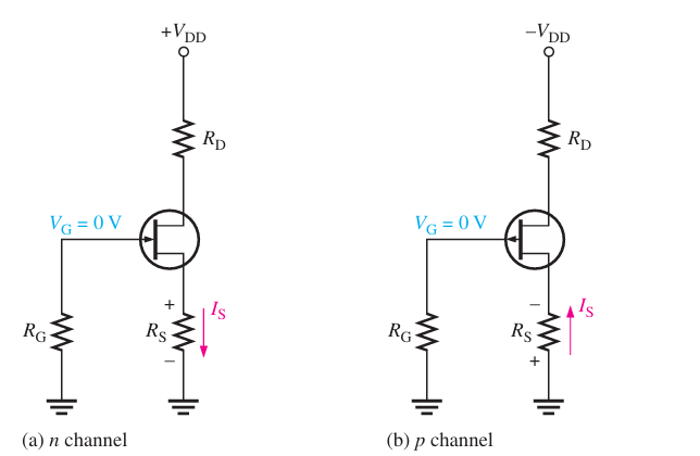

Why do we have RG if it has no effect in the circuit
Force the gate to be 0V and isolate AC signal from ground in amp application
What are the two ways of setting the Q-point of a self-biasing JFET
Use the transfer characteristic curve for a particular JFET (Use this when some values are unknown)
Use Shockley's equation (More practical)
How to use the transfer characteristic curve to find the Q-point
Get the gate voltage
Get two points
First point → Where ID = 0A
Second second point → Where VGS = 0V
Get the line equation (if needed)
Find the point of intersection (This is your Q-point)
If I want to do a midpoint bias, what should by ID and VGS should be
ID = 0.5IDSS and VGS = VGS(Off) / 3.4
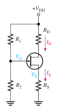
Draw a circuit of a voltage-divider bias (JFET)
What are the two types of MOSFET we do?
Enhanced MOSFET
Depletion MOSFET
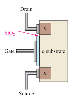
What is the difference between JFET and MOSFET
The gate of the MOSFET is insulated from the channel by a silicon dioxide layer
What is the difference between FET and BJTs
FETs are unipolar devices while BJTs are bipolar devices
BJTs are current controlled devices while FETs are voltage controlled
JFETs have a very high input impedance while BJTs do not
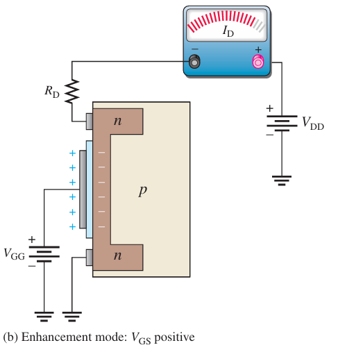
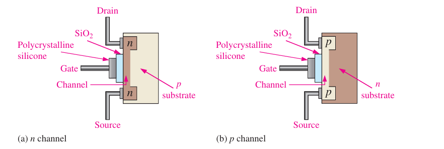
Draw a basic construction of a E-MOSFET
What mode does E-MOSFET operate in
Only in enhancement mode
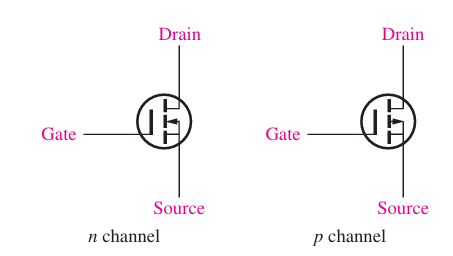
Draw schematic symbol for E-MOSFET
Draw a basic structure of D-MOSFET
What mode does D-MOSFET work in?
Enhancement and depletion
What makes D-MOSFET able to have positive and negative voltage apply to the gate
The gate is insulated from the channel
Draw the E-MOSFET transfer characteristic curve
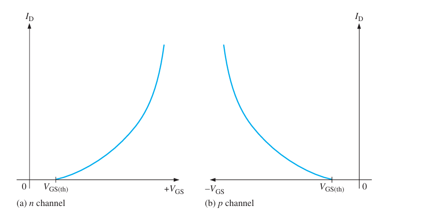
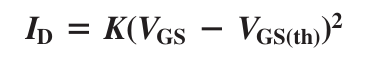
What is the formula for the E-MOSFET characteristic curve?
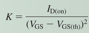
How do you find K for the E-MOSFET
Draw the D-MOSFET characteristic curve
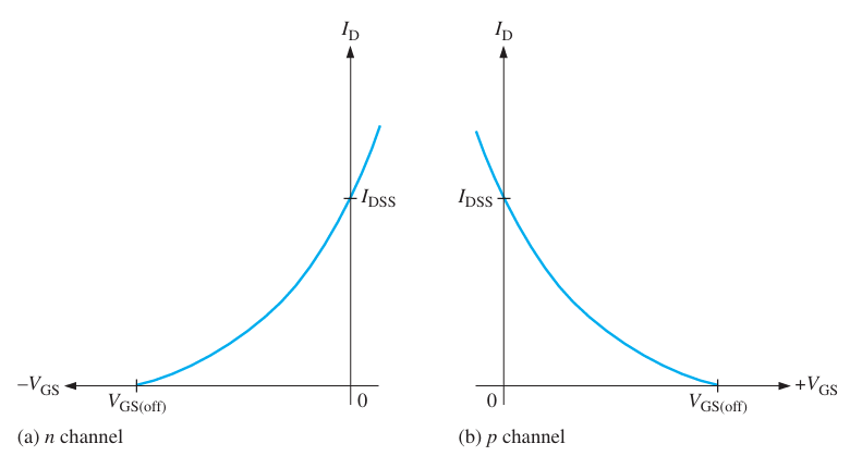
What is the formula for the D-MOSFET
Same as the JFET
Why is E-MOSFET useful and common in IC applicaiton
Simpler construction
Used in digital ICs
What are the two biasing configuration for E-MOSFET
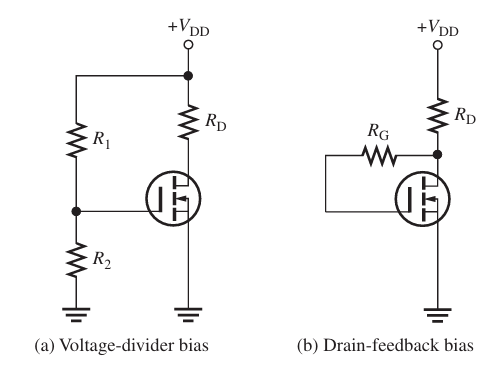
What is the gate voltage for a drain-feedback bias?
VGS = VDS
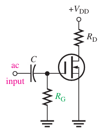
Why is there RG ?
It allows AC signal to develop at the gate (isolating it from ground)
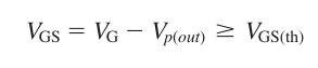
Draw n-channel MOSFET as a switch
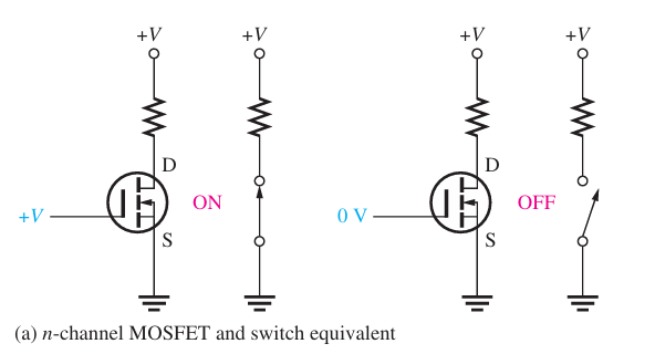
Draw p-channel MOSFET as a switch
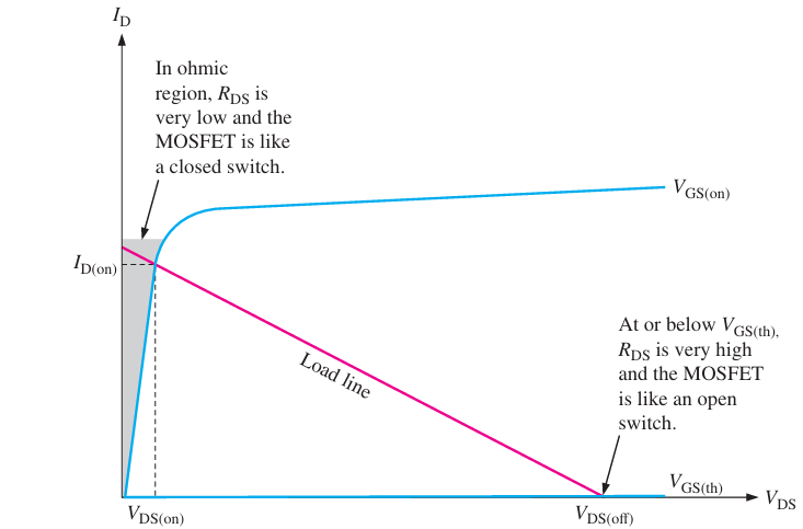
Draw an ideal switching operation load line on the drain characteristic curve
What is one thing you need to make sure when you applying an AC signal at the gate?
Ensure the signal level at the source must not cause the VGS to drop below the VGS(th)
Draw a basic operation of a n-channel MOSFET analogue switch
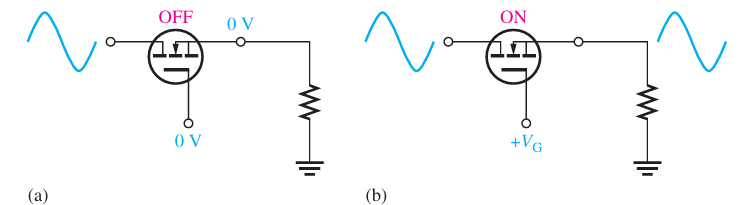
Draw a sampling circuit and input & output waveform
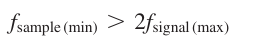
What is the Nyquist frequency
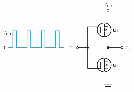
Draw a CMOS
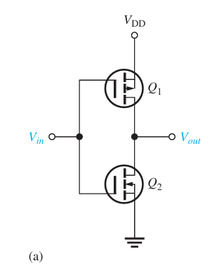
What type of gate is a CMOS?
NOT Gate
What is the main advantage of CMOS?
Consume very little DC power
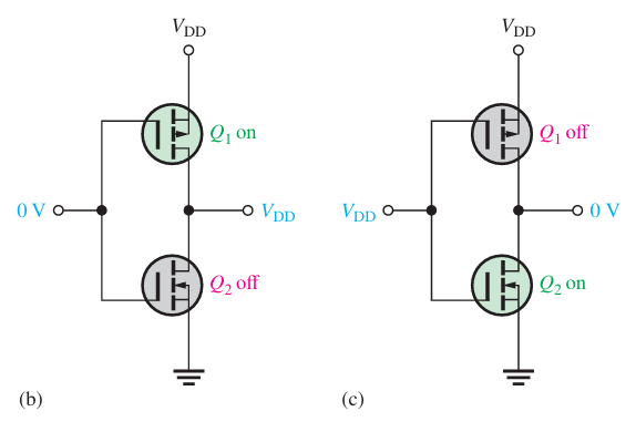
Draw the two state of a CMOS
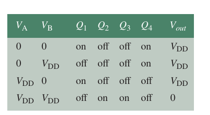
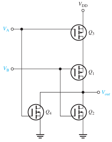
Draw a CMOS NAND gate
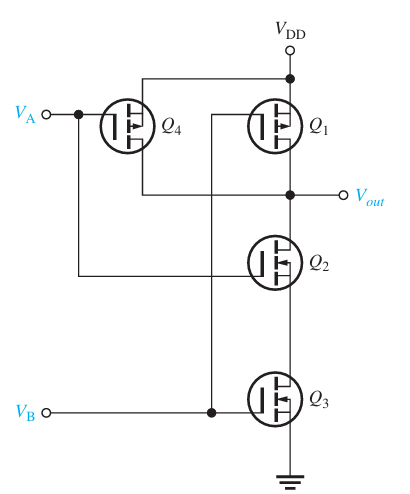

Draw a truth table for this
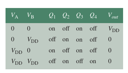
Draw a CMOS NOR

Draw a truth table for this
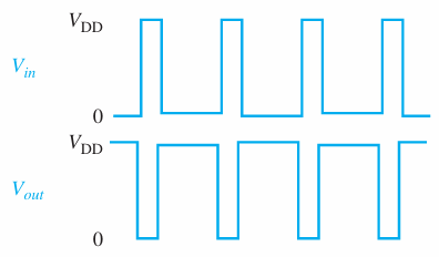
What will the output wave be for this?
What is the purpose of a buffer?
It means that we can provide a high input impedance "buffer" between the input and output to provide some electrical isolation between parts of the circuit, for example between a low power logic circuit and a high-power motor circuit
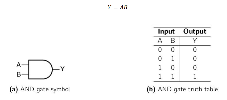
Draw the gate symbol, truth table and expression for AND gate
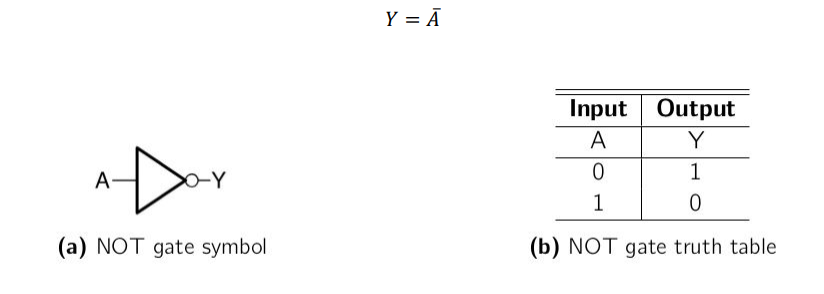
Draw the gate symbol, truth table and expression for NOT gate
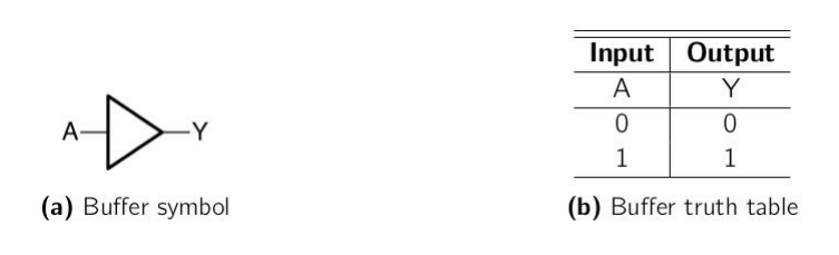
Draw the gate symbol, truth table for Buffer
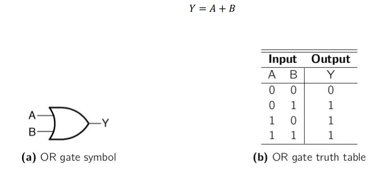
Draw the gate symbol, truth table and expression for OR gate
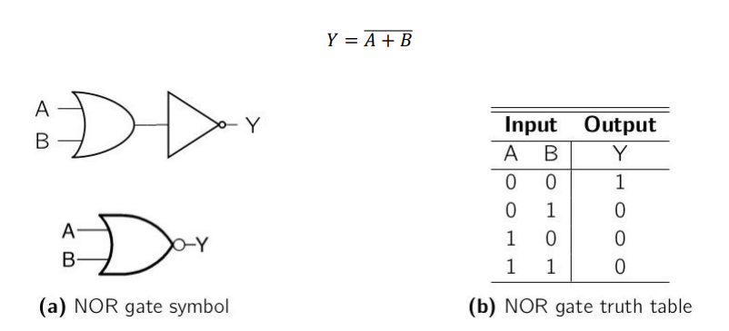
Draw the gate symbol, truth table and expression for NOR gate
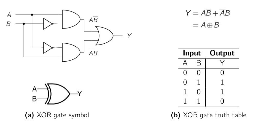
Draw the gate symbol, truth table and expression for XOR gate
What happens to the current for MOSFET switching on each rising and falling edge?
A huge spike in current due to the internal capacitive behaviour of the MOSFET
Draw a diagram of D-MOSFET in depletion mode
Draw a diagram of D-MOSFET in enhancement mode