PhD
 Call Kai
 Learn
Learn Practice Test
 Spaced Repetition
 Match
Match Flashcards
 Knowt Play
1/44

There's no tags or description
Looks like no tags are added yet.
Name | Mastery | Learn | Test | Matching | Spaced | Call with Kai | Chat |
|---|
No analytics yet
Send a link to your students to track their progress
45 Terms
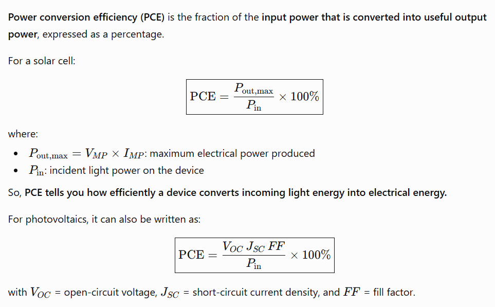
PCE
how much can photon up conversion improve solar cells and is it worth it in terms of efficiency vs price?
That is a very relevant question. For silicon solar cells, the gain from photon upconversion is expected to be rather modest, because silicon already absorbs a large part of the solar spectrum up to around 1100 nm. For example, even if we assume a broadband upconversion system with 5% efficiency, which has not yet been realized, the power conversion efficiency of a silicon solar cell would only increase by about 1 percentage point.
However, the concept becomes more interesting for higher-bandgap materials. These materials absorb a smaller part of the solar spectrum, so they lose more low-energy photons. If those photons can be upconverted into usable light, the relative efficiency gain could be much larger.
So at this stage, I would not claim that upconversion is or will be commercially competitive for silicon solar cells. The value of this project is more fundamental and enabling: improving the absorber materials and device concept so that upconversion can become more efficient, low-cost and applicable not only in photovoltaics, but also in sensing, imaging and photocatalysis
Eg. TiO2 absorbs UV photons for water splitting
How does NIR imaging work and what role do UCs play in this application?
NIR light penetrates tissue better than visible light because tissue generall absorbs and scatters it less strongly. You can therefore shine NIR light onto or into tissue and detect the light that was not absorbed. Different molecules absorb different NIR wavelengths to different extents, so the detected NIR intensity contains information about the tissue composition. By recording where light comes from and/or which wavelengths are absorbed, you can build an image.
Upconverting nanoparticles inside the body
You illuminate the body with NIR light. Because NIR penetrates relatively deeply, it can reach particles that would be difficult to excite directly with visible light. The particles absorb the NIR photons and emit visible light, so their location appears as a bright region in the image. If the particles are specifically targeted toward cancer cells, their emission could indicate where the tumour is located.
An upconverting foil outside the body
Imagine light passing through or reflecting from the body and reaches a conformal UC layer following th body’s shape. The tissue creates spatial NIR intensity pattern accoriding to its absorption. The UC foil converts that invisible NIR pattern into a visible pattern that can be detected with a convential affordable Si camera. So the foil acts as a NIR-to-visible imaging screen.
Advantage
you can also covert NIR directly with NIR cameras but these are costly and thus hinder the development of new low-end applications as well as the vast application potential of NIR imaging
current camera’s = InGaAs
UC properties to realise these applications
low-cost
large area
lightweight
mechanically compliant
efficient broadband UCs
current progress in UCs
current UCs are not ready for the practial realization of these applications
they do not have the mentioned properties
and don’t have sufficient UCQY
Dye-sensitized lanthanide-doped nanoparticles
UCQY: up to 5% only at high intensity laser irradiation of 10 W/cm² within a narrow absorption band
TTA (triplet-triplet annihilation
UCQY of a few precent at >10 W/cm² and wavelenths < 900 nm
TTA and lanthanide-doped nanoparticles are non linear?
Dye-sensitized lanthanide-doped nanoparticles or triplet-triplet annihilation rely on photophysical events involving at least 2 excited states
In a linear process:
If you double the light intensity, you roughly double the emitted light.
But in many upconversion systems, especially lanthanide- or TTA-based systems:
If you double the light intensity, the emitted upconverted light may increase much more than twofold — or, at low intensity, may be very weak.
This happens because the process often needs two excitation events or two excited states to interact before one higher-energy photon can be emitted.
So at low light intensity, the chance that these required excited-state events happen close enough in time is small. Therefore, the upconversion quantum yield drops strongly.
organic diode-based approach
consisting of device stacks where a photodetector (PD) drives a light-emitting
diode (LED). An external voltage is required and compensates for the difference in photon energy.
Advantage
scales linearly with incident light intensity
allows pixel less imaging
Disadvantage
external voltage needed
introduces extra noise
external electrical energy consumption, so not suitable for solar energy applications
organic diode based solution
PD-stack = stacking two or more PDs
the PD stack delivers a sufficiently high voltage to drive the LED
This concept was demonstrated in 2018 using two GaAs PDs monolithically integrated and short-circuited with a GaInP LED, achieving 810 nm to VIS up-conversion at a quantum yield of 1.5%.[5] However, elaborate lithography for pixelation is still required here.
pixel-less imaging
Limited lateral movement of the charge carriers, recombination thus occurs within a few 100 nm of where the photons was absorbed
Compared to pixel-based imaging, pixel-less organic upconversion is not primarily designed to digitally record or process an image. Instead, it directly converts an incoming NIR image into visible light across a continuous organic film. This avoids pixel patterning and readout electronics, making it attractive for thin, flexible, and large-area NIR visualization.
For example for night-vision or biomedical imaging
in organic diode base upconversion where does the additional energy of the emitted photon come from?
The extra energy comes from the electrical energy generated by multiple absorbed NIR photons in the stacked photodetectors. The voltages generated in each OPD layer add up and drive the OLED, so the emitted higher-energy photon is powered by the combined energy harvested from several lower-energy photons, not by a single NIR photon alone.
Breakthrough UHasselt
novel approach using a vertical stack of several organic PDs and an organic LED
UCQY >1% at low intensities <10 mW/cm²
was measured outcoupled to air
The outcoupling factor from organics on glass substrates with an effective refractive index of 1.4-1.5 is approximately 0.25, which means that the effective internal UCQY is on the order of 4%.
The prototype UC stack does not require any external voltage to achieve NIR to green up-conversion and already outperforms other approaches at low light intensities
How does PD stack generate own photovoltage?
In one OPD, the NIR absorber, for example a BODIPY donor material, absorbs a photon and reaches an excited state. In that excited state, an electron can be transferred from the donor LUMO to the acceptor LUMO, such as C₆₀.
So:
the electron moves into the acceptor phase and is transported toward the electron transport layer / cathode side
the hole remains on the donor/BODIPY phase and is transported toward the hole transport layer / anode side
Because electrons and holes are separated in opposite directions, a voltage difference builds up across the OPD. This is the photovoltage.
The reason a deep HOMO is important is that the photovoltage is strongly related to the energy difference between the donor HOMO and the acceptor LUMO:
A deeper, lower-lying HOMO gives a larger energy difference to the acceptor LUMO. This allows the separated electron–hole pair to store more electrical energy, giving a higher photovoltage.
So the design challenge is:
The main design challenge is to combine long-wavelength NIR absorption with sufficient photovoltage.
A deep donor HOMO is needed to generate a high photovoltage, which helps reduce the number of OPD layers in the stack. Fewer layers are preferred, because although more OPDs increase the total voltage, they also split the absorbed photons over more subcells, reducing the maximum current and limiting visible emission.
The trade-off is that a deeper HOMO generally leads to a larger HOMO–LUMO gap, which limits the achievable red-shift.
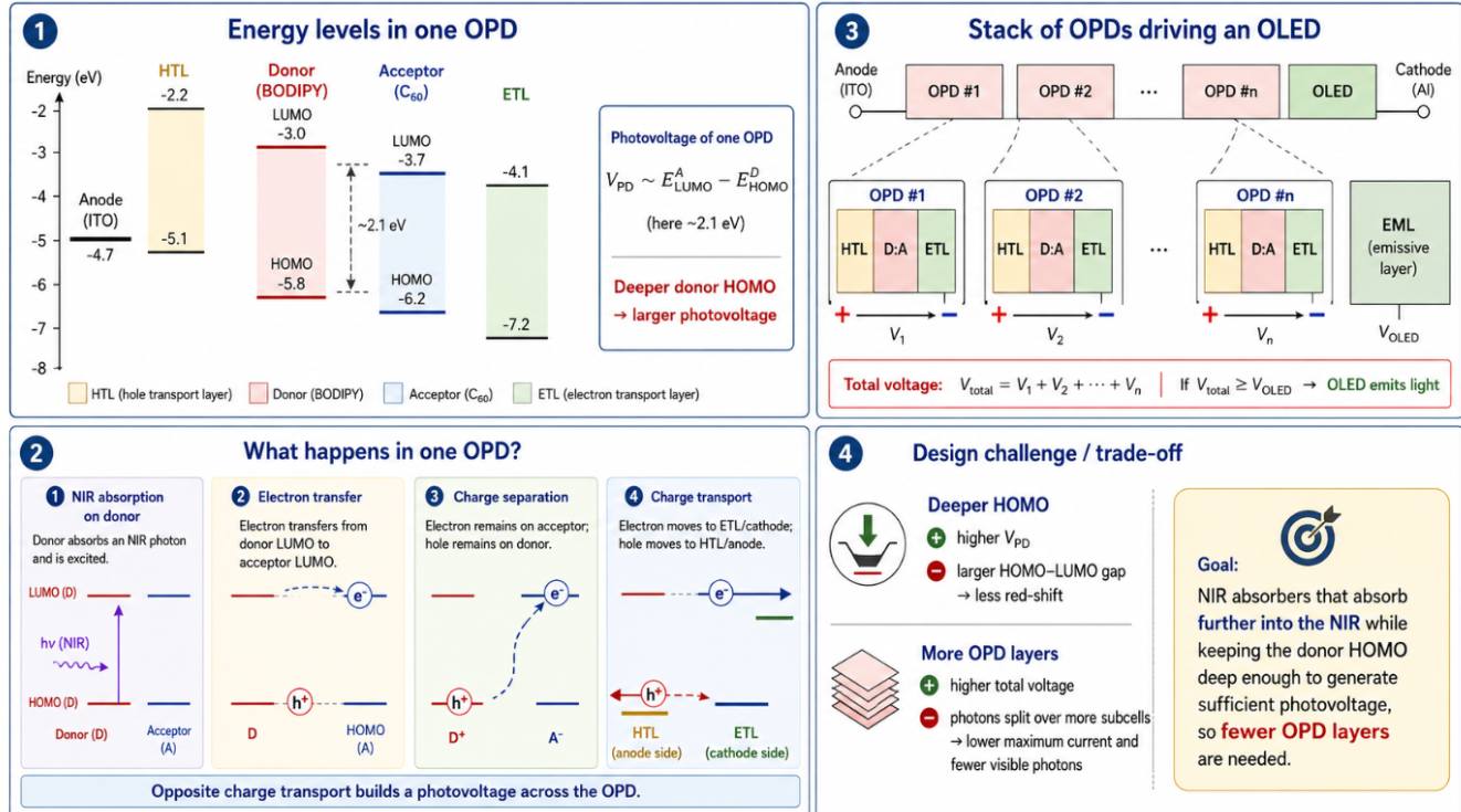
but then it seems like in OPD1, there's now an electron in the HOMO of the donor while electrons should move in the LUMO of the acceptor. So my question is, an electron moves in the LUMO of the acceptor and a hole in the HOMO of the donor after excitation, but how do they move after they enter the next layer?
I think in OPD1 and OPDn you see the electron moving to the cathode and the hole to the anode, and electrons and holes in between are a sort of electric interconnection, they do not move explicitly but ensure the whole process is connected.
working principle organic UC stack
Upon illumination with low-energy photons, the PDs generate electrons (●) and holes (○). These recombine at the junctions between the PDs and in the LED material. The current density (J) flowing through the shorted device runs through each of the elements. Care must therefore be taken that the generated photocurrent by each of the sub-PDs is matched, i.e., all layer thicknesses need to be optimized such that an equal fraction of the incident photons is absorbed by each sub-cell. A stack of N PDs must deliver a sufficient photovoltage, N×VPD, to drive the LED, with VPD the photovoltage produced by a single PD. A high UCQY thus requires an LED with a low driving voltage (VLED, related to the energy of the emitted photons) and PDs with a high VPD (related to the longest absorbed wavelength). Reducing the number of PDs improves the UCQY, as it increases the fraction of absorbed photons in each sub-PD. Utilizing a stack of 4 PDs, as in the exploratory study, limits the internal UCQE to 25% (6–8% exter-nal UCQE when outcoupling to air), whereas this would rise to 50% if 2 PDs generate sufficient voltage.
advantages of UC stack (13)
Thin-film architecture
Organic UC stacks can be made as very thin devices, which makes them lightweight and compact.Mechanical flexibility
Organic semiconductors are less brittle than many inorganic semiconductors and can potentially be used on flexible substrates.No strict lattice matching required
Organic layers do not need to have the same crystal structure or atomic spacing as the layer underneath. This makes it easier to combine different materials in one stack.Broader material choice
Because lattice matching is not a major limitation, different absorber, transport, and emitter materials can be selected more freely.Low-cost fabrication potential
Organic layers can be deposited using scalable techniques such as vacuum deposition, printing, or solution processing.Lower material consumption
Thin-film deposition uses very small amounts of active material compared with bulk semiconductor fabrication.Potentially lower CO₂ footprint
Organic thin-film processing can be less energy-intensive than high-temperature inorganic semiconductor processing.Use of OLED technology
The visible-emitting part of the UC stack is based on OLEDs, which are efficient, bright, and highly tunable.Tunable emission colour
The emitted visible colour can be controlled by choosing the appropriate organic emitter.Pixel-less imaging possible
A continuous UC film can locally convert an incoming NIR image into visible light without needing predefined pixels.Large-area compatibility
Organic thin films are well suited for large-area devices and surfaces.Good performance at low light intensities
Organic photodetectors can be highly sensitive, making the UC stack suitable for weak NIR signals.Integration potential
Organic UC stacks can potentially be integrated into lightweight, flexible, or wearable imaging systems.
Reducing the number of PDs improves the UCQY
Each PD only generates current from the photons it absorbs. Since the PDs are in series, the LED current cannot be the sum of all PD currents. It is limited to the current that can flow through the whole stack.
magine 100 photons enter a stack of 4 PDs. Each PD absorbs about 25 photons. Because the 4 PDs are in series, their voltages add:
But the current does not add. The same current flows through all 4 PDs. So the LED current corresponds roughly to the current from 25 photons, not 100 photons.
So the ideal internal UCQE limit is about ¼ = 25% for 4 PDs
Trade off: More PDs give more voltage, but they divide the absorbed photons over more sub-cells, which reduces the maximum possible current — and therefore limits the number of visible photons that can be produced.
Overall UC project research objectivse
Expand wavelength
Solar powered photocatalytic > 800 nm
Imaging > 1000 nm
because the longer the wavelength, the lower energy light we need and the more cost efficient the process is
and for imaging and sensing: Night vision, biomedical sensing requires longer wavelengths
Improve internal UCQY beyond 20 % at intensities < 10 mW/cm²
The light intensity of the sun at the Earth's surface on a clear day is approximately 100 mW/cm².
Previously: Utilizing a stack of 4 PDs, as in the exploratory study, limits the internal UCQE to 25% (6–8% exter-nal UCQE when outcoupling to air
Prototype has an internal UCQY of around 4% when taking losses such as photons outcoupled to air, it becomes a little over 1%
2018 PD stack had a UCQY of 1.5%
Characterize the stacks for performance, stability, linea-rity, dynamic range, response time, and noise
Investigate the potential for (i) imaging > 1000 nm, by integrating an UC and a low-cost camera, and (ii) Improving photocatalysis by integrating UCs in a lab-scale solar photocatalytic system.
aims PhD within overall UC program
The presented Ph.D. project fits in this broader, interdisciplinary, organic UC program and aims in particular at the development of novel, more efficient NIR absorbers for the OPD devices in the stack
objectives:
Rational synthesis of organic molecules with strong NIR absorption and suitable frontier molecular orbital energies that can still be vacuum-evaporated, taking full benefit of the most important advantage of organic dyes, i.e., the fact that their electro-optical properties can be readily tailored.
Thorough structural and photophysical characterization of the novel organic absorbers.
Evaluation of the novel organic molecules in prototype OPD stacks.
Smooth integration of the NIR OPD work in the overarching organic UC program.
Project dissemination and valorization, while committing to Open Science practices.
- Is dit allemaal wel haalbaar voor één student? Ben jij voldoende beslagen in computationele chemie en device-fysica?
Computationally: Tom cardinaals heeft dit gedaan voor de phase 1 BODIPY’s, maar hij is er nu niet meer. Het is mogelijk dat Joline dit gaat doen, zo niet moeten we nog kijken om het het waard is om de tijd te steken in mij op te lijden om die berekeningen te doen gezien alle andere dingen die ik moet doen. Maar gezien mijn computationele achtergrond moet dat geen probleem zijn;
IUMAT
IUMAT staat voor het Instituut voor Materiaalonderzoek
requirements for OPD active materials
Absorption in the NIR >750 nm
High molar absorptivity
Minimal absorption in the emission window of the LED - avoid reabsorption
Because the led light goes again through the PD layers in the stack
Deposit materials by evaporation - restricts size and mass of the absorber
frontier molecular orbital energy levels
higher HOMO is lower voltage in the photodetector which may be insufficient to drive the LED, so extra PD layers are required
But a lower HOMO increases the HOMO-LUMO gap, restricting absorbtion in the NIR
a lower LUMO lowers the LUMO-LUMO offset with the acceptor material
design restrictions
Higher HOMO is lower voltage in PD → requires more PDs to generate sufficient voltage to drive the LED
Voltage: V = E/q with E = energy available, q = charge of one electron
So if a photodiode creates separated charges, the maximum voltage it can produce is linked to the energy difference between the charges after separation. The HOMO-LUMO energy difference tells you how much electrical energy one separated electron–hole pair can provide.
A larger donor-HOMO to acceptor-LUMO energy difference gives each separated charge pair more electrical energy, which can result in a higher photovoltage.If the donor HOMO is raised, that energy difference becomes smaller, so the photovoltage decreases.
Lower LUMO
More susceptible to oxidative degradation??? → mistake
Lowers the required offset to the electron acceptor material in the photodiode
In an organic photodiode, after the absorber absorbs light, the excited electron has to be transferred from the absorber to an electron acceptor.
For this electron transfer to happen efficiently, the acceptor LUMO usually needs to be lower in energy than the absorber LUMO. The energy difference between them is the LUMO–LUMO offset.
“Lowering the absorber LUMO can reduce the LUMO–LUMO offset needed for electron transfer to the acceptor. This may help limit voltage losses, provided that the remaining offset is still sufficient for efficient charge separation
BODIPYs
characterized by narrow and intense absorption centered around 500 nm, but the optical gap can be lowered via synthetic strategies. The DSOS group also has wide experience with them and they’re tunable, photostable and allows deposition by evaporation.
novel 4H-furo[3,2-b]pyrrole BODIPY derivatives with stronger donor substituents will be prepared, staying close to the BDP-OMe ‘lead’ structure but envisaged to shift the absorption beyond 800 nm (in film).
(OMe had abs of 723nm (sol.), 800 nm (film)
QC calculation predict stronger donor substituents cause an additional bathochromic shift along with a rise of the HOMO energy
Change the accepting group at the meso position: to maximize the absorption red-shift
switch to the Aza-BODIPY variants
absorption more red-shifted but tedious synthesis
The QC analysis is used to assess trends rather than absolute values
the 3 BODIPYs with the largest red-shift will be synthesised first
TPA: triphenylamine
JUL: julolidine
NMe2: dimethylamine
![<p>characterized by narrow and intense absorption centered around 500 nm, but the optical gap can be lowered via synthetic strategies. The DSOS group also has wide experience with them and they’re tunable, photostable and allows deposition by evaporation.</p><p></p><ol><li><p>novel 4H-furo[3,2-b]pyrrole BODIPY derivatives with stronger donor substituents will be prepared, staying close to the BDP-OMe ‘lead’ structure but envisaged to shift the absorption beyond 800 nm (in film).</p><ol><li><p><span style="background-color: transparent;"> (OMe had abs of 723nm (sol.), 800 nm (film)</span></p></li></ol></li><li><p>QC calculation predict stronger donor substituents cause an additional bathochromic shift along with a rise of the HOMO energy</p></li><li><p>Change the accepting group at the meso position: to maximize the absorption red-shift</p></li><li><p>switch to the Aza-BODIPY variants</p><ol><li><p>absorption more red-shifted but tedious synthesis</p></li></ol></li></ol><p>The QC analysis is used to assess trends rather than absolute values</p><p>the 3 BODIPYs with the largest red-shift will be synthesised first</p><ul><li><p>TPA: triphenylamine</p></li><li><p>JUL: julolidine</p></li><li><p>NMe2: dimethylamine</p></li></ul><p></p>](https://assets.knowt.com/user-attachments/0a9d05ab-c1f9-4bfa-9562-fb9e05bdc72a.png)
why do donor substituents on BODIPY systems lower the optical gap?
Electron-donating substituents usually raise the HOMO energy more strongly than they raise the LUMO. As a result, the HOMO–LUMO gap becomes smaller.
n BODIPY systems, donor groups can also increase π-conjugation and promote intramolecular charge-transfer character, especially when combined with electron-poor parts of the molecule. This stabilizes the excited state and further lowers the transition energy.
how does this donor acceptor character help?
In a normal π–π* transition, the electron is excited within roughly the same part of the molecule.
In a donor–acceptor system:
the donor part is electron-rich
the acceptor part is electron-poor
after excitation, electron density shifts partly from donor to acceptor
This charge-transfer excited state is often lower in energy than a purely local excited state.
lower excited-state energy⇒smaller optical gap⇒longer-wavelength absorption
synthesis of furopyrrole BODIPY derivatives
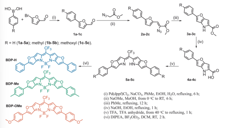
alternative synthetic strategy starting from commercial methyl 4H-furo[3,2-b]pyrrole-5-carboxylate (made from furfural, a bio-based chemical derived from lignocellulose). This protocol has already been (successfully) tested in a student project up to the dipyrromethene stage
Since the literature approach toward BDP-OMe introduces the donor substituent in the first step,[16,17]and the yield for the furopyrrole fusion is particularly low,
![<p><span style="background-color: transparent;">alternative synthetic strategy starting from <strong>commercial </strong>methyl 4H-furo[3,2-b]pyrrole-5-carboxylate (made from <strong>furfural</strong>, a bio-based chemical derived from lignocellulose). This protocol has already been (successfully) tested in a student project up to the dipyrromethene stage</span></p><p><span style="background-color: transparent;">Since the literature approach toward BDP-OMe introduces the donor substituent in the first step,[16,17]and the yield for the furopyrrole fusion is particularly low,</span></p><p><br></p>](https://assets.knowt.com/user-attachments/ef2b2adb-48d4-4e5c-a1ce-259741139dca.png)
Previous procedure furopyrrole BDPs
problem: donor substituent is introducted in the first step and has low fusion yield
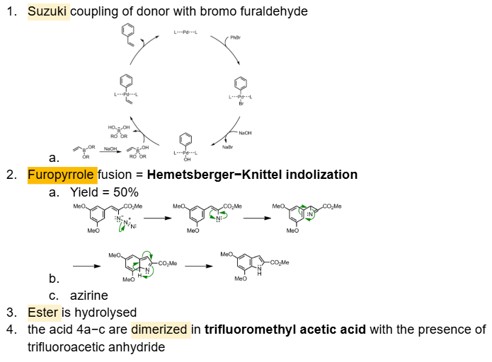
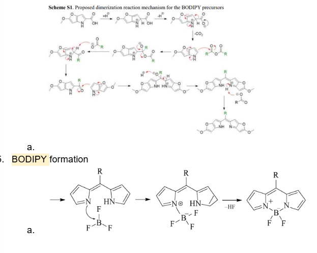
synthesis of other BODIPY derivatives
the same strategy as previously applied will be used
computational screening
compound selection
critical evaluation of the synthetic protocol and revising it where deemed useful
synthesis and purification
Alternatives
thienopyrrrole-fuesd BODIPY dyes with various meso substituents
Aza-BODIPY variants (look most promising)
thienopyrrole fused
beta fused
alfa-beta linked
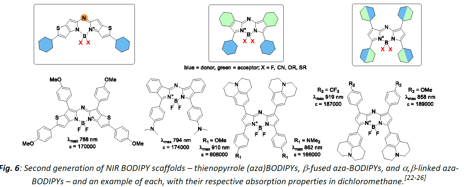
GOAL = achieve desired properties rather than developing new organic reactions
synthesis of Aza BODIPYs
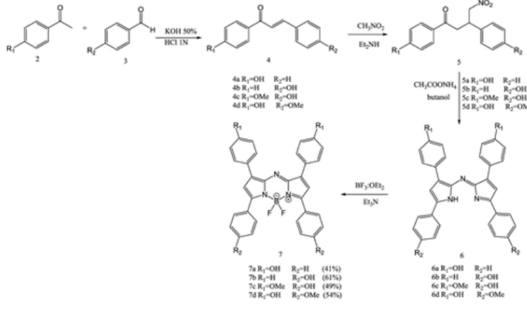
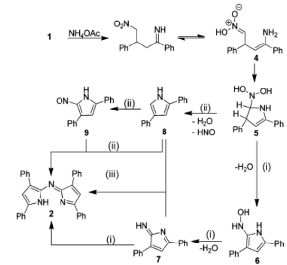
The aza-BODIPY compounds (7a, 7b, 7c, and 7d) were synthesized as described in Figure 1, starting with the Claisen-Schmidt condensation reaction of different acetophenones (2) and benzaldehydes (3) to obtain the corresponding chalcones (4) to subsequently carry out a Michael reaction with the addition of the nitro group (nitromethane) in the β proton of the chalcone (5), followed by the synthesis to obtain the aza-dipyrromethenes (6) using ammonium acetate in butanol, which were finally reacted with triethylamine and BF3·EtO2 Boron trifluoride etherate for the synthesis of aza-BODIPYs (7).
characterization of all compounds
NMR, MALDI, FTIR
Need high purity to avoid charge traps and dark currents in the PD devices which lead to lower photovoltages and thus lower performance. Insufficient purity could also lead to contamination of the evaporation equipment
Thus new molecules will undergo extensive purification
Thermal properties and stability needed for vacuum sublimation will be determined by scanning calorimetry and thermogravimetric analysis
scalability
only need a 100 mg of the final compound after sublimation to allow proper evalutaion of the suitability of the material
Challenge WP1
Create small NIR absorbers with high extinction coeff, that can be evaporated, mix well with complementary acceptor and show a sufficiently deep HOMO to generate sufficient photovoltage
You need a deep HOMO because the photovoltage of an organic photodetector is largely determined by the energy difference between the donor HOMO (BODIPY) and the acceptor LUMO (eg. C60)
Design challenge: need higher HOMO to lower gap to absorb lower E photons but also sufficiently deep to generate a large enough photovoltage
Alternative to BODIPYs
(na)phtalocyanines, have shown absorbtion up to 1000 nm and for which absorption can be tuned by:
changing the metal ion
ring extension
changing substituents
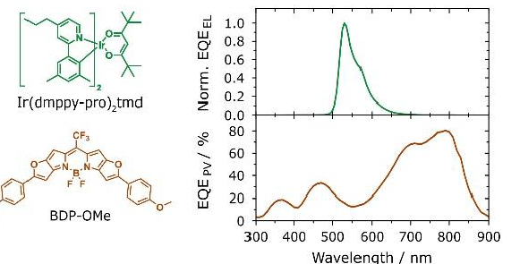
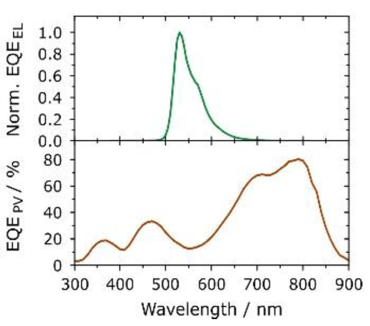
what is the green compound
the emitter in the OLED, green light (530 nm)
WP2: computational, photophysical and electrochemical characterization
The envisaged molecules will be subjected to quantum chemical calculations: (density functional theory, DFT) (supervised by prof. B. Champagne and his team)
The allows to select the most promising materials in terms of excitation energies, oscillator strengths, HOMO-LUMO levesl, etc. before engaging in compound synthesis
Champagne has previously compared various exchange-correlation functionals in terms of their performance to describe experimentally relevant excited state properties of NIR BODIPY derivatives
highly accurate wavefunction methods are in general beyond reach for the compounds of interest
determining the experimental photophysical properties
We will determine:
absorption spectra
extinction coefficients
fluorescence in solution and thin film
These results will be compared with the QCs
Extinction coefficients
need > 5×10^4 cm-1 to maximize the photon to electron conversion yield and absorb as much light as possible in thin films
Identify non-radiative decay pathways
via spectrally and time-resolved fluorescence measurements combined with photoluminescence quantum efficiency measurements
this can be linked to the max achievable photovoltage of the synthesised materials
Stability
assess via photostability tests under UV illumination to guarantee sufficient stability for device integration
HOMO-LUMO levels
via cyclic voltammetry eventhough they are only estimates
when more accurate results are needed, UPS (ultraviolet photoelectron spectroscopy) can be considered
All combined data will provide feedback for adjusting and developing new design concepts in WP1
film thickness
Films will be 30-60 nm thick
But thickness needs to be optimized, so each absorbs equal amount of photons, to have an equal currentdensity throughout the system
This is similar to tandem solar cells:
The lowest-current subcell limits the current of the whole stack.
Although each organic layer is only tens of nanometres thick, a stacked OPD contains many layers. The upper OPDs absorb part of the incoming NIR light, so the photon flux reaching deeper OPDs is reduced. Therefore, the subcells do not automatically receive equal photon flux. Since the OPDs are connected in series, the total current is limited by the subcell that generates the lowest photocurrent. The stack must therefore be optically designed for current matching, using layer thickness, absorber strength, transparent interconnection layers, and optical interference control to ensure that each OPD contributes a similar photocurrent while still generating enough total voltage to drive the OLED.