LP architecture final exam
1/50
There's no tags or description
Looks like no tags are added yet.
Name | Mastery | Learn | Test | Matching | Spaced | Call with Kai |
|---|
No study sessions yet.
51 Terms
answer i
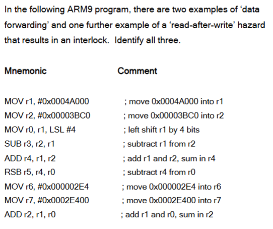
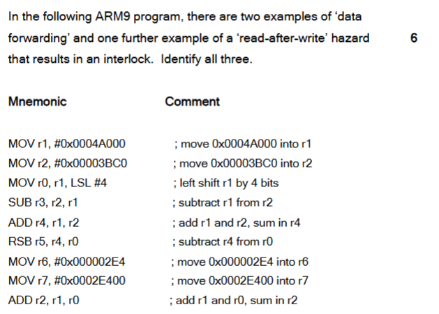
A read-after-write hazard occurs because an instruction may attempt to read a register before a previous instruction has written the correct result back to that register.
In a pipelined processor, multiple instructions overlap in execution. In the ARM9 5-stage pipeline, register operands are read at the end of the Decode stage, while results are written back in the Write-back stage. If an instruction produces a result that is written to a register in stage 5, and the immediately following instruction needs that register as a source operand, then the second instruction will read the register in stage 2 before the first has written the updated value. As a result, the second instruction reads an old value, creating a RAW hazard.

answer ii
Data forwarding (also called bypassing) eliminates the RAW hazard by routing the result of an instruction directly from a later pipeline stage to an earlier stage, without waiting for the value to be written back to the register file.

answer iii
An interlock is a hardware mechanism that detects a pipeline hazard and automatically stalls the pipeline until the hazard is resolved.
When forwarding cannot supply the required data in time, the interlock prevents the dependent instruction from advancing.
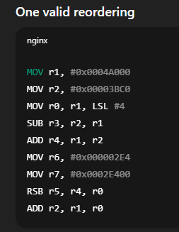
Data forwarding
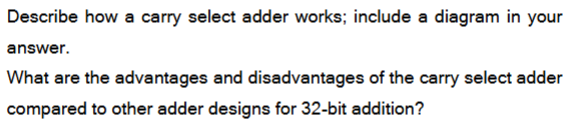
MOV r1, #0x0004A000→MOV r0, r1, LSL #4
The second instruction requires the value of r1 before it has been written back. The result from the first instruction is therefore forwarded directly to the execute stage.MOV r2, #0x00003BC0→SUB r3, r2, r1
TheSUBinstruction uses r2 immediately after it is produced by theMOV. The value of r2 is supplied via data forwarding rather than waiting for write-back.
RAW hazard causing an interlock
ADD r4, r1, r2→RSB r5, r4, r0
TheRSBinstruction depends on the result in r4 produced by the immediately precedingADD. This dependence cannot be fully resolved by forwarding alone in the ARM9 pipeline, so a pipeline stall (interlock) is inserted to ensure the correct value is used.
Draw a pipeline diagram for the program given assuming that it is executed using the ARM9 microprocessor
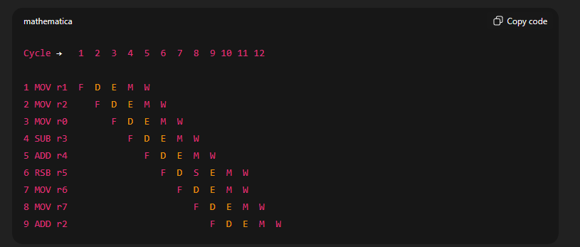
M does not take place as none of the instructions access the memory

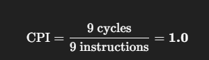
What is the performance, as measured in ‘clocks per instruction’ (CPI)? (counting clock cycles from the execute stage of the first instruction to the execute stage of the last instruction)
How can the instructions be reordered so that ‘read-after-write’ hazard do not occur without changing the function of the programme?
The interlock is caused by the dependence between instructions 3 and 6 on r0.
This can be eliminated by moving independent instructions between them, without changing program behaviour.
The two MOV instructions (to r6 and r7) do not depend on r0 or r4 and allow sufficient time for r0 to be written back, eliminating the interlock.
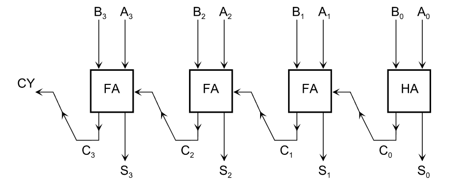
Modern microprocessors are typically designed so that the clock period is less than 10 gate delays. With reference to this, explain why a 32-bit addition cannot be implemented using a traditional ripple carry adder. Your answer should include a diagram of part of a ripple carry adder (not all 32-bits).
A 32-bit ripple carry adder cannot meet this requirement because the carry signal propagates serially from the least significant bit to the most significant bit. Each bit position uses a full adder, and the carry-out of one full adder is used as the carry-in to the next. In the worst case, a carry generated at the LSB must pass through all 32 full adders before the final sum is valid.
Since each full adder introduces several gate delays, the total carry propagation delay increases linearly with word size and is far greater than 10 gate delays for a 32-bit adder.
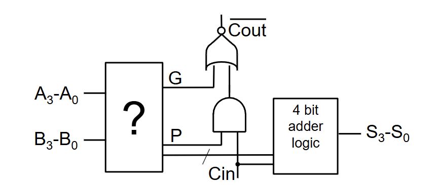
Instead of allowing the carry to ripple through each bit, carry signals are computed in parallel using combinational logic.
For each bit, two signals are generated from inputs A and B:
the generate signal (G), which is set when a carry is produced (A = 1 , B = 1).
the propagate signal (P), which is set when an incoming carry will be passed on (A ⊕ B = 1).
The carry-out is then computed as:
Cout = G + P ⋅ Cin
This allows the carry to be determined without waiting for bit-by-bit propagation, and the resulting carry is supplied directly to the adder to produce the sum outputs.
Compared to a ripple carry adder, a CLA is much faster, since carry delay does not increase linearly with word length.
However, the CLA requires extra hardware to generate carry logic, increasing area, power consumption, and design complexity.
A carry select adder (CSA) improves addition speed by pre-computing results for both possible carry-in values and selecting the correct result once the actual carry is known.
For each block, the inputs A[3 : 0] and B[3 : 0] are applied to two parallel adders that compute:
sum0[4:0], assuming the carry-in is 0sum1[4:0], assuming the carry-in is 1
Each result includes both the sum bits and the carry-out. A multiplexer, controlled by the actual carry-in, selects the correct output to produce the final sum[3:0] and Cout.
Because both results are computed in advance, the CSA avoids waiting for carry propagation through the entire block. The critical path is limited to the carry from the previous block plus the multiplexer delay.
For a 32-bit adder built from multiple blocks, a CSA is much faster than a ripple carry adder, since carry propagation is confined to block boundaries. Compared to a carry look-ahead adder, it has simpler and more regular hardware.
The main disadvantage is increased area and power consumption, as each block requires duplicated adder logic and multiplexers.
![<p>A <strong>carry select adder (CSA)</strong> improves addition speed by <strong>pre-computing results for both possible carry-in values</strong> and selecting the correct result once the actual carry is known.</p><p>For each block, the inputs <span>A[3 : 0]</span> and <span>B[3 : 0] </span>are applied to two parallel adders that compute:</p><ul><li><p><code>sum0[4:0]</code>, assuming the carry-in is 0</p></li><li><p><code>sum1[4:0]</code>, assuming the carry-in is 1</p></li></ul><p></p><p>Each result includes both the sum bits and the carry-out. A <strong>multiplexer</strong>, controlled by the actual carry-in, selects the correct output to produce the final <strong>sum[3:0]</strong> and <strong>C<sub>out</sub></strong>.</p><p>Because both results are computed in advance, the CSA avoids waiting for carry propagation through the entire block. The critical path is limited to the <strong>carry from the previous block plus the multiplexer delay</strong>.</p><p>For a 32-bit adder built from multiple blocks, a CSA is <strong>much faster than a ripple carry adder</strong>, since carry propagation is confined to block boundaries. Compared to a carry look-ahead adder, it has <strong>simpler and more regular hardware</strong>.</p><p>The main disadvantage is <strong>increased area and power consumption</strong>, as each block requires duplicated adder logic and multiplexers.</p>](https://knowt-user-attachments.s3.amazonaws.com/932b3a61-a667-4dfd-af2d-8e40330cea3c.png)

answer i
answer ii

answer iii
A carry propagate adder produces a final result by propagating carries from one bit position to the next, so its delay depends on the carry chain length.
A carry save adder does not propagate carries immediately. It adds three operands and produces a sum and a carry vector, storing carries for later use.
In the ARM7 multiplier, carry save adders are used to accumulate partial products without carry propagation, reducing delay.

It is important to know whether the operands are two’s complement (signed) or unsigned because the most significant bit has a different meaning in each format.
For unsigned integers, all bits contribute only to the magnitude, whereas for two’s complement numbers the MSB represents the sign and negative values are encoded differently.
When calculating a double-length 64-bit product, the multiplier must treat sign bits correctly. For signed multiplication, sign extension is required so that negative operands produce a correct 64-bit result. If the wrong number format is assumed, the upper 32 bits of the product will be incorrect.
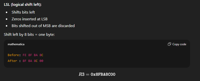
Multiplication by 2n is achieved using a logical shift left (LSL #n). Each left shift moves all bits left by one position, multiplying the value by 2. For example, LSL #3 multiplies a number by 23
Division by 2n is achieved using a right shift. For unsigned numbers, a logical shift right (LSR #n) divides the value by 2n. For signed (two’s complement) numbers, an arithmetic shift right (ASR #n) is used so that the sign bit is preserved.
An MMU performs address translation by converting a program’s virtual address into a physical memory address.
The virtual address is divided into a page number and an offset. The MMU uses the page number to look up a page table entry, which provides the base address of the physical page. The offset is then added to form the physical address.
Address translation is useful because it enables memory protection, allows multiple applications to share memory safely, and supports virtual memory, where the virtual address space can be larger than physical memory.
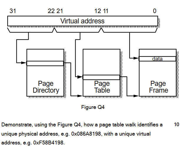
The virtual address is divided into three fields:
Bits 31–22: page directory index
Bits 21–12: page table index
Bits 11–0: page offset
Using the example virtual address 0xF58B4198, the top 10 bits (31–22) are first used to index the page directory. This lookup identifies the base address of the corresponding page table in physical memory.
Next, the middle 10 bits (21–12) of the virtual address are used as an index into this page table. The selected page table entry contains the base address of a physical page frame, along with any associated attributes.
Finally, the bottom 12 bits (11–0) of the virtual address form the offset within the page. This offset is added to the physical page frame base address to produce the unique physical address, for example 0x086A8198.
Page table walking increases memory access time because multiple memory accesses are required to translate a virtual address.
In a two-level page table, three memory accesses are needed: one to read the page directory entry, one to read the page table entry, and one to access the actual data. This significantly increases the memory access latency compared to a single physical memory access.

A Translation Look-Aside Buffer (TLB) decreases memory access time by caching recently used virtual-to-physical address translations.
When the CPU generates a virtual address, the MMU first checks the TLB. On a TLB hit, the physical address is obtained immediately, avoiding a page table walk and reducing the number of memory accesses to one. On a TLB miss, the page table walk is performed and the translation is then stored in the TLB.
Programs tend to repeatedly access the same virtual pages (temporal locality) and nearby addresses within the same page (spatial locality).
Because of this locality, recently used address translations stored in the TLB are likely to be reused, resulting in a high TLB hit rate.
For a typical TLB with 64 entries, a hit rate of about 99% can be achieved, even with a relatively small number of entries.
Describe Von Neumann architecture and its advantages and disadvantages
A von Neumann architecture uses a single memory and a single bus for both instructions and data. Instructions and data share the same address space and cannot be accessed simultaneously.
The advantage of the von Neumann architecture is its simple design and lower hardware cost, but it suffers from the von Neumann bottleneck, where instruction fetch and data access compete for the same bus.
Describe Harvard architecture and its advantages and disadvantages
A Harvard architecture uses separate memories and separate buses for instructions and data, allowing instruction fetch and data access to occur at the same time.
The advantage of the Harvard architecture is higher performance due to parallel access, but it has increased hardware complexity and cost.
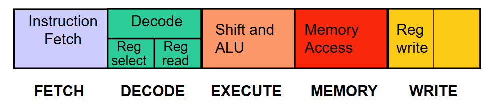
An instruction pipeline improves processor performance by overlapping the execution of multiple instructions. Each instruction is divided into stages such as fetch, decode, execute, memory access, and write-back, with different instructions occupying different stages simultaneously.
Once the pipeline is full, the processor can complete one instruction per clock cycle, increasing throughput compared to a non-pipelined processor where instructions execute sequentially.
Increasing the number of pipeline stages can further improve performance because each stage performs less work, allowing the clock period to be reduced. This enables a higher clock frequency, increasing the number of instructions executed per second.
i)
ARM9 includes additional instructions not present in ARM7, such as CLZ. These instructions allow certain operations to be performed with fewer instructions, reducing the total number of instructions executed for a program.
ii)
ARM9 uses a deeper, more advanced pipeline than ARM7, with improved data forwarding and hazard handling. This reduces pipeline stalls and allows closer to one instruction per cycle for many instruction sequences, lowering the average CPI compared to ARM7.
iii)
The ARM9 pipeline is designed with shorter pipeline stages, reducing the critical path delay. This allows the processor to operate at a higher clock frequency than ARM7, increasing fclk.
EOR R1, R1, R2
Stores R1 ⊕ R2 in R1.
EOR R2, R1, R2
Recovers the original value of R1 into R2.
EOR R1, R1, R2
Recovers the original value of R2 into R1.
This code swaps the contents of registers R1 and R2 using the exclusive OR (EOR) operation, without using any additional CPU registers.
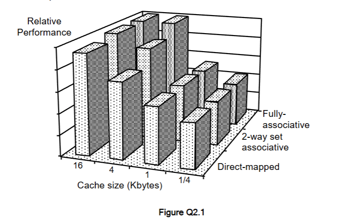
Figure Q2.1 shows the relative performance of three different cache designs at four different sizes of cache memory assuming that the clock frequency of the cache memory is 2.5 times greater than the main memory clock frequency. Briefly explain the difference between a direct mapped cache, a 2-way set associative cache and a fully associative cache.
A direct-mapped cache maps each block of main memory to one fixed cache line. It is simple and fast but suffers from a high number of conflict misses, as different memory blocks can map to the same line.
A 2-way set associative cache divides the cache into sets with two lines per set. A memory block can be placed in either line of the indexed set, reducing conflict misses compared to a direct-mapped cache, at the cost of extra tag comparison hardware.
A fully associative cache allows a memory block to be stored in any cache line. This minimises conflict misses and gives the highest hit rate, but requires complex comparison logic and a replacement policy, increasing hardware cost and power consumption.
A direct-mapped cache has the lowest performance because each memory block maps to only one cache line, causing many conflict misses.
A 2-way set associative cache allows each block to be placed in two possible lines, reducing conflict misses and improving the hit rate.
A fully associative cache allows a block to be placed in any cache line, minimising conflict misses and therefore achieving the highest hit rate and best performance for the same cache size.
i)
Occurs because data accessed once is likely to be accessed again a short time later. An example of this is a counter in a loop, which is accessed repeatedly over a short period. Once the counter is brought into the cache, subsequent accesses are fast hits.
ii)
Occurs because data from one memory location is likely to be accessed if data in an adjacent memory location has been recently accessed. An example of this is when a program accesses an array in order. When array 0 is accessed, the cache often brings in the subsequent arrays into a cache line, anticipating they will be needed soon.
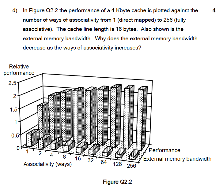
As the ways of associativity increase, a given memory block has more possible cache locations, so there are fewer conflict misses than in a direct-mapped or low-associativity cache. Fewer misses means the processor needs to fetch fewer cache lines from main memory and performs fewer external memory transactions. Therefore the external memory bandwidth requirement decreases as associativity increases, because more accesses are satisfied by the cache (higher hit ratio, lower miss ratio).

In a write-through cache, every write to the cache is immediately written to main memory as well. This keeps main memory always up to date and simplifies consistency, but it increases external memory traffic and bandwidth usage.
In a copy-back cache, data is written only to the cache, and main memory is updated later, when the cache line is evicted. A dirty bit is used to indicate modified cache lines. This reduces memory traffic and improves performance, but requires more complex control logic and can make memory coherence more difficult.
i) Dynamic voltage and frequency scaling (DVFS)
Dynamic voltage and frequency scaling reduces power consumption by lowering the supply voltage and clock frequency when full performance is not required.
ii) Dynamic power dissipation
Dynamic power dissipation is the power consumed when transistors switch state during circuit operation.
iii) Leakage power dissipation
Leakage power dissipation is the power consumed due to leakage currents in transistors, even when the processor is idle or not switching.
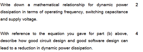
P=C f VDD2
Good circuit design reduces dynamic power by lowering the effective switching capacitance C, for example through careful layout, smaller transistor sizes, and clock gating to reduce unnecessary switching.
Good software design reduces dynamic power by lowering the switching activity and operating frequency f, for example by reducing instruction count, avoiding unnecessary memory accesses, and allowing the processor to run at lower frequencies or enter low-power modes.
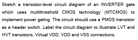
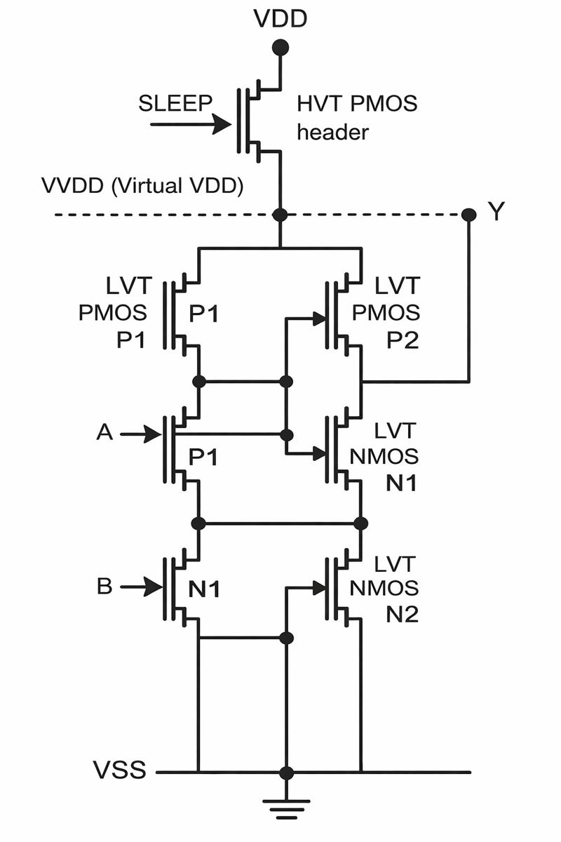
(i) Working of the circuit
The inverter uses LVT PMOS and NMOS transistors for high performance and is supplied by a virtual VDD. A HVT PMOS header transistor connects the real VDD to the virtual VDD.
When the header transistor is ON, virtual VDD equals VDD and the inverter operates normally. When the header is OFF, virtual VDD is disconnected from VDD, effectively powering down the inverter and reducing standby current.
(ii) Why MTCMOS with LVT and HVT reduces leakage power
LVT transistors have high performance but high leakage, while HVT transistors have low leakage. MTCMOS combines these by using LVT devices in the logic and an HVT device as a sleep transistor. Turning off the HVT header during standby cuts off the leakage path to VDD, greatly reducing leakage power while maintaining high performance when active.
A virtual address is the address generated by the CPU for a program. It is part of the program’s virtual address space and does not directly correspond to a location in physical memory.
A physical address is the actual address used to access main memory (RAM). It identifies the real location of data in physical memory after address translation.
A page table is a data structure used by the MMU to translate virtual addresses into physical addresses. It maps virtual pages to physical page frames and contains additional control information such as access permissions.
A memory protection unit (MPU) assigns attributes to regions of memory to control how they are accessed. Typical attributes include read/write permissions, privilege level, executable or non-executable, and cacheability and bufferability of the memory region.
A memory address may be assigned as uncacheable when it corresponds to locations that can change independently of the CPU, and caching them could cause the processor to read stale or incorrect data or delay writes. Marking these regions uncacheable ensures that all accesses go directly to the device and occur in the correct order.

Virtualization is the technique of allowing multiple operating systems or applications to run on the same physical hardware by presenting each with its own virtual view of the processor, memory, and devices. Hardware resources are shared while remaining isolated from each other.
A hypervisor is a software layer that manages virtualization. It controls access to the physical hardware, allocates resources to each virtual machine, and ensures isolation between them.
A stack is a LIFO memory structure, with data added by push and removed by pop, and the current top tracked by the stack pointer.
On a subroutine call, the return address, saved registers, and local data are pushed onto the stack. When the subroutine returns, this information is popped so execution resumes correctly.
For nested subroutines, each call saves its own context on the stack. Because the stack is LIFO, returns occur in the reverse order of calls, ensuring correct program execution.
describe the term power gating
Power gating reduces leakage power by disconnecting idle circuit blocks from the power supply using a sleep transistor. When the circuit is not in use, the sleep transistor is turned off, isolating the logic from VDD or VSS and reducing leakage current. When active, the transistor is turned on to allow normal operation.
Clock gating is a low-power technique in which the clock signal is disabled to parts of a circuit when they are not in use, preventing unnecessary switching.
By stopping the clock, flip-flops do not toggle and the associated combinational logic remains static, reducing switching activity, which is the main source of dynamic power dissipation.
Latched clock gating is preferred because it prevents glitches on the gated clock. The enable signal is latched when the clock is low, so it cannot change during the high phase of the clock.
This avoids spurious or short clock pulses that could occur in non-latched gating if the enable changes while the clock is high. As a result, latched clock gating provides safe, reliable clock control and reduces dynamic power consumption.
When adding instructions to an instruction set, designers must consider how frequently the operation is used, whether it reduces instruction count, and the hardware cost and complexity required. The effect on the pipeline, control logic, verification effort, and software compatibility must also be assessed.
The main advantages are fewer instructions for common operations and possible performance and energy improvements, since complex operations can be executed in a single instruction.
The main disadvantages are greater instruction set and hardware complexity, increased area and power consumption, and longer design and verification time. Some added instructions may be rarely used, limiting their benefit.
Major features omitted or reduced in Thumb include:
Conditional execution on most instructions.
Flexible second operand with barrel shifter.
Full access to all registers.
Complex addressing modes.
Some specialized and complex instructions available in ARM mode.
In Thumb mode, the processor fetches 16-bit Thumb instructions from memory. In the instruction decode stage, each Thumb instruction is decompressed into an equivalent 32-bit internal ARM instruction.
This decompressed instruction has the same format as a normal ARM instruction and is then passed through the standard ARM pipeline and execution units. As a result, no separate Thumb execution hardware is required.

The Thumb instruction set is designed to improve code density by using 16-bit instructions instead of 32-bit ARM instructions. This reduces program size and instruction fetch bandwidth.
Thumb achieves this by using simpler instructions, fewer addressing modes, and limited register access.
Thumb code is advantageous in memory-constrained and low-power embedded systems, where reduced code size lowers memory usage and power consumption.

The semantic gap is the difference between high-level language constructs and the machine-level instructions of a processor. A smaller semantic gap means machine instructions more closely match high-level operations.
Code density measures how much functionality is achieved per unit of memory. Higher code density means smaller programs and reduced instruction fetch bandwidth.

A larger cache has better performance because it can store more memory blocks, which reduces the cache miss rate. With fewer misses, the processor needs to access main memory less often, reducing average memory access time.

The disadvantages of a larger cache are increased hardware area and cost, higher power consumption, and potentially longer cache access time due to increased size and complexity. These factors can limit clock frequency and reduce the overall performance benefit of a very large cache.

In a copy-back cache, data is written only to the cache and main memory is updated only when a modified cache line is evicted. This reduces the number of write accesses to main memory, thereby reducing the external memory bandwidth requirement compared to a write-through strategy.
Power gating reduces leakage power by using a high-threshold-voltage (HVT) PMOS header transistor to disconnect idle logic from VDD, creating a virtual VDD.
When the circuit is active, the header transistor is on, so virtual VDD is connected to VDD and the logic operates normally. When the circuit is idle, the header transistor is off, isolating the low-threshold-voltage (LVT) logic transistors from the supply.
This prevents leakage current from flowing through the LVT devices, and because the HVT transistor has low leakage, the overall standby leakage power is greatly reduced.