Intro to Bipolar Junction Transistors & DC Analysis
1/42
There's no tags or description
Looks like no tags are added yet.
Name | Mastery | Learn | Test | Matching | Spaced | Call with Kai |
|---|
No analytics yet
Send a link to your students to track their progress
43 Terms
pn junction biasing
a pn junction is under biasing when an external voltage is applied across the p and n regions, controlling whether charge carriers can cross the junction
biasing means connecting a voltage source so one side of the semiconductor is at a higher potential than the other → modifies the depletion region
forward biasing lowers the barrier and lets current flow
reverse biasing raises the barrier and suppresses current until breakdown
forward biasing on a pn junction
the p side is made more positive than the n side
the depletion region narrows, which lowers the voltage barrier that obstructs carrier diffusion
results in the majority of the carriers being able to cross the junction between p and n easily, producing a large current once the applied voltage approaches the pn junction’s threshold
how to forward bias a pn junction / diode
connect the battery positive to the diode’s anode (p side) and the battery negative to the cathode (n-side)
how to reverse bias a pn junction / diode
connect the battery positive to the cathode (n side) and the negative to the anode (p side) → almost no current thru the junction unless the reverse voltage is large enough to cause breakdown
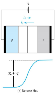
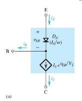
visual of reverse biasing a pn junction (explain it)
depletion region widens
the bottom graph shows the electrostatic potential energy (barrier voltage) across the pn junction
the curve’s maximum point is equal to the built-in voltage V0 (present with no external bias) PLUS the reverse voltage Vg that was applied
diode current (ID) is very small under reverse biasing and is roughly constant until breakdown
saturation current (IS) is larger than ID but not by much considering ID is super small
what is ID (diode current) ?
the current flowing thru the diode terminals (dir is from anode to cathode) in the circuit
follows the diode equation → in forward bias, ID is positive and rises exponentially the more voltage applied, and is very small and approx constant negative current in reverse bias until the breakdown region
what is IS (saturation current)?
a small temperature-dependent constant that represents the diode’s leakage current scale
comes from minority carriers (electrons and holes freed due to thermal ionization) that diffuse across the junction when no forward bias is applied
about minority carriers: electrons generated on the p side are pulled across to the n side OR holes generated on the n side are pulled across to the p side
sets the baseline current in the diode eqn and dets how much reverse leakage current you get
always “positive”
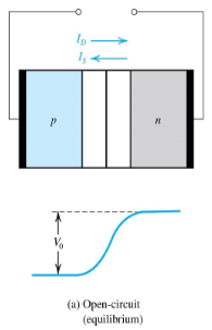
visual of having no external biasing on a pn junction (explain it)
V0 is the built-in voltage barrier
depletion region is neither big or small
ID and IS are about the same since the pn junction is at equilibrium
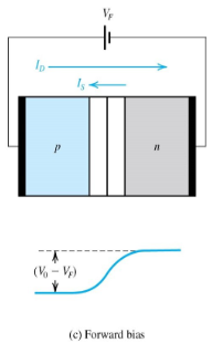
visual of having forward biasing on a pn junction (explain it)
positive side of the battery is applied to the p side of the pn junction, which makes the p-side more positive
more holes diffuse from the p side to the n side, creating positive diode current across the junction
the biasing lowers the barrier voltage (V0 - VF)
simplified structure of npn transistor
simplified structure of pnp transistor
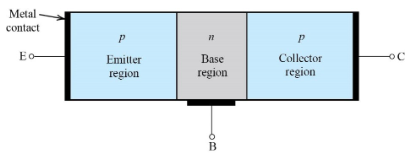
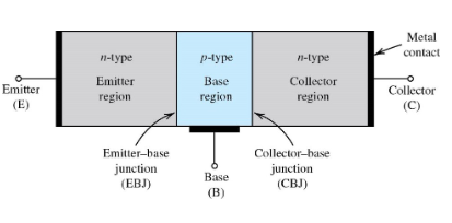
structure of bjt transistor
made of three layers of p-type/n-type material (npn or pnp)
has three terminals: emitter, base, and collector
emitter: like a water source that pushes a lot of tiny balls (charge carriers)
base: is a thin gate; a small current at the base terminal opens the gate
collector: when the gate is open, the big current exits the transistor thru the collector terminal
the way the emitter, base, and collector work together means that a small base current controls a larger collector current, which is how the transistor amplifies a small input signal (current or voltage) into a larger output.
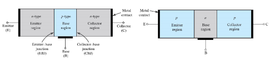
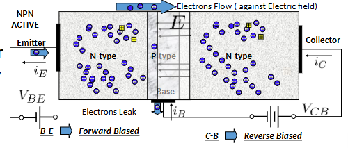
how current moves through an npn transistor
the net CONVENTIONAL current (which tracks the movement of holes) goes from collector to emitter
majority carrier: electrons that travel from emitter → base → collector
when the base-emitter junction is forward biased, the n-type emitter injects electrons in the p-type base, and the electrons then cross the reverse-biased base-collector junction to the n-type collector, producing a large collector current
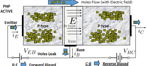
how current moves thru pnp
the net conventional current moves from emitter to collector
majority carrier: positive holes that travel from emitter to base to collector
the p-type emitter injects positive holes into the n-type base (the base emitter junction is in forward bias) and the holes then travel to the collector (base-collector junction is reverse biased)
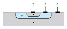
simplified structure of what a bjt transistor actually looks like in practice
E B C in that order
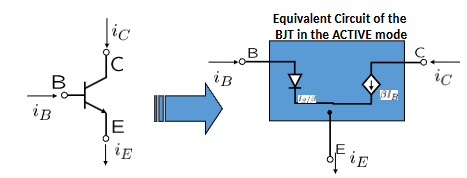
operation modes of a transistor: active (or forward active) mode
where the transistor behaves as a linear amplifier
base-emitter junction is forward biased and base-collector junction is reverse biased
in the active mode, a small change in the base current or base-emitter voltage produces a much larger change in the collector current (exactly what you expect from a linear amplifier)
this is the mode needed for DC and AC analysis
this is the only mode where the equations for IC and IE associated with a transistor are valid
operation modes of a transistor: reverse active mode
the transistor is driven so the collector and emitter basically switch roles → the base-emitter junction is reverse biased and the base-collector junction is forward biased
functions poorly as an amplifier compared to the forward active mode
operation modes of a transistor: cutoff mode
the transistor’s OFF state
both junctions (base-collector or base-emitter) are reverse biased → conducts no collector current and behaves like an open circuit
occurs when the base-emitter voltage VBE is below the forward threshold (0.7) so the emitter can’t inject carriers into the base
operation modes of a transistor: saturation mode
both junctions (EB and CB) are forward biased
device behaves like a closed switch and the collector current cannot be increased much by increasing the base current
check that VBE is forward and VBC is also forward
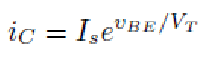
exponential law equation for collector current in the active mode
iC = DC collector current flowing from collector to emitter (npn) or from emitter to collector (pnp) in forward-active operation
IS = saturation current, is an intrinsic property so can’t be found through mathematical analysis
vBE = base-emitter voltage → potential difference between the base and emitter terminals that forward biases the base-emitter junction
VT = thermal voltage, can use 25.85 mV
what is base current made up of ?
“electronics” → electrons
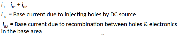
you inject ____ in the base for npn and inject ____ in the base for pnp
electrons; holes
for npn, the conventional base current flows ____ the base terminal
for pnp, the conventional base current flows ____ the base terminal
into
out
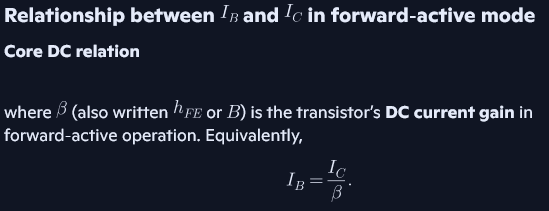
in forward-active mode, what is the relationship between IB and IC?
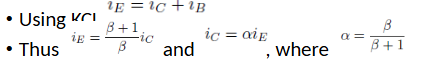
in forward-active mode, what is the relationship between IE and IB?
IE = (beta + 1)IB
in forward-active mode, what is the relationship between IE and IC?
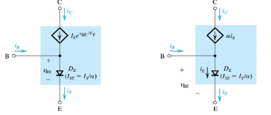
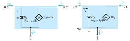
npn active-mode models for common-base circuits
npn active-mode models for common-emitter circuits
common-base circuit
input is applied between emitter and the base
output is taken between the collector and the base
base is held at the AC ground via bias network or direct ground
usually high voltage gain
low current gain
common-emitter circuit
the input is applied between the base and emitter and the output is taken between the collector and emitter
the emitter is often tied to a reference ground (maybe with a resistor in the branch)
high voltage gain
high current gain
common collector circuit
input is applied to the base and the output is taken from the emitter (usually across an emitter resistor or load)
high current gain
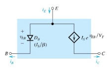
pnp active-mode model for common-base circuits
pnp active-mode model for common-emitter circuits
npn transistor equivalent model
npn transistor charge carrier mpvement
pnp transistor equivalent model
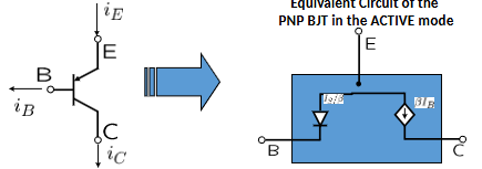
pnp transistor charge carrier
for DC analysis, you should assume _____________
active mode unless otherwise mentioned or active mode conditions are violated
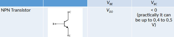
active mode conditions for npn transistor
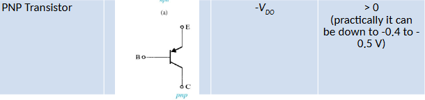
active mode conditions for pnp transistor
VBE should be -VDO
VBC should be greater than 0
DC currents can’t be ______ in active mode
negative
if the currents are negative, then you should consider another mode like cutoff mode where the currents = 0
what does “performing DC analysis” for a circuit including a transistor mean?
finding every DC voltage at the terminals of the transistor (VE, VB, VC) and finding all the currents that travel thru the transistor (IE, IB, IC)
in DC analysis, it’s advised to start with the KVL loop that includes _____
VBE (or VEB) since you know it equals 0.7 in active mode