Nanofab Final Exam
1/46
There's no tags or description
Looks like no tags are added yet.
Name | Mastery | Learn | Test | Matching | Spaced | Call with Kai |
|---|
No analytics yet
Send a link to your students to track their progress
47 Terms
Integrated Circuit (IC)
a circuit in which the electrical elements are embedded in a single semiconductor substrate and inseperable from it. In modern use, this substrate is a semiconductor wafer, most frequently made of silicon, and the electrical elements are microscopic.
Translator
a semiconductor device used to amplify or switch electrical signals and power. Transistors are capable of very simple functions that are at the core of digital processing. E.g. change a 1 to a 0. Transistors can be discrete or part of an integrated circuit.
Semiconductor
A material for which it is possible to change the conductivity/ resistivity over many orders of magnitude. For our purposes, this is done mainly by doping but conductivity/resistivity is also a function of temperature.
Free charge carrier
an electron or a hole that is available to create a current
Field Effect Transistor (FET)
A transistor that switches on and off due to the electric field created by ther gate voltage making a channel.
Complementary Metal Oxide Semiconductor (CMOS)
The standard way of making logic circuits since the 1960's. NMOS and PMOS transistors occur in pairs and any input signal will turn one of them off and one of them on. N pairs of these are made to implement a logical function. N>= 1.
Aerial Image
in the context of photolithography, the aerial image is the light pattern at the top of the photoresist
Thermal Oxidation of Silicon
The process of exposing silicon in a wafer to a source of oxygen, in a heated furnance, to create a layer of SiO2.
Etch Selectivity
the comparison of etch rates between two materials. Material 1 is the material one desires to etch. Material 2 is in the vicinity of material 1 and the intention is that the etching of material 2 is minimized.
Directionality or anisotropy
a qualitative or quantitative term that addresses whether the etching method/recipe causes etching
Parasitic
In reference to electrical circuits, this is resistance, capacitance, or inductance that is unwanted and is not intentionally designed into the circuit. The goal is to minimize these.
Shot Noise
the unwanted statistical fluctuations, pulse to pulse, of the number of photons produced by the exposure system
Line Edge Roughness (LER)
The deviation of a feature edge (as viewed top-down) from a smooth, ideal shape.
Piezoelectricity
the phenomenon in which mechanical stress is reated in a body/material when a voltage is applied to it.
Reverse Piezoelectricity
the phenomenon in which mechanical stress is created in a body/material when a voltage is applied to it.
Micro-electro-mechanical-systems (MEMS)
Technology of microscopic devices incorporating both electronic and moving parts. Devices are typically 10's to 100's of microns.
Sensor
A system that detects and responds to multiple physical inputs and converts them into analogue or digital forms. Sensors enable perception.
Actuator
A device that converts and electrical signal to a physical signal, motion, force or torque. Actuators produce action/movement.
Dennard Scaling
Also called "ideal scaling". All dimensions of the chip shrink linearly at the same rate. This worked for decades but is no longer possible.
Strained silicon
A technique to improve mobility of charge carriers by intentionally mismatching lattice constants of two crystals, with one crystal being silicon for our purposes. This causes the Si lattice constant to increase or decrease compared to its normal value. The strain changes charge carrier mobility.
Silicon on Insulator (SOI)
An integrated iruit manufacturing approach that aims to more completely isolate the transistor channel to achieve specific performance gains.
FinFET
A 3D transistor in which one or more channels are controlled by the gate on three sides. The channel(s) is/are shaped like the fin of a fish.
Gate All Around (GAA)
A 3D transistor in which one or more channels are controlled by the gate on three sides. The channel(s) is/are shaped like the fin of a fish.
Backside Power
An IC manufacturing approach where the back end of line wiring is split so that the signal wiring is on one side of the wafer and the power delivery is on the other side.
Leakage Current
current in an IC that flow when it is not supposed to and/or where it is not supposed to.
The number of transistors on a chip (latest record holder)
100 billion
The approximate size of the smallest feature made, intentionally, on a wafer in full manufacturing today, using EUV lithography
10 nm
Atomic density in pure crystal:
5 x 10^22 atoms/cm^3
Size of the band gap of a pure silicon crystal at room temperature:
1.1 eV
Wavelengths of Deep Ultraviolet light used in semiconductor photolithography:
248 nm and 193 nm
Wavelengths of Extreme Ultraviolet light used in semiconductor photolithography:
13.5 nm
Cost of a current EUV system:
$400 million
[10] Number of alternating layers in a Mo/Si EUV reflective photomask:
45
What is the best description of what is shown?
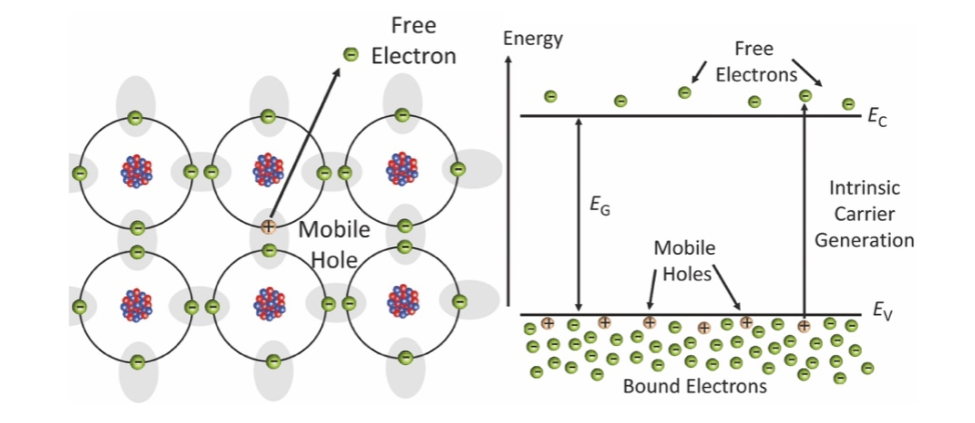
For a pure intrinsice semiconductor, at a temperature above absolute zero, the number of free electrons in the conduction band is equal to the number of mobile holes in the valence band. Intrinsic free electrons and mobile holes are produced as a pair. And, if they recombine, the recombine as a pair. So, for intrinsic silicon, “n” is always equal to “p”.

What is the desription of what happens at absolute zero and above absolute zero?
At absolute zero, there would be no free electrons with energies above Ec and there would be no mobile holes below Ev. As the temperature increases from absolute zero to room temperature, more and more pairs of free electrons and mobile holes are created from the available thermal energy. The probability of creating such a pair is quite small, but this probability increases with temperature. Also, there are many atoms per cubic centimeter, so the overall effect is significant.
What does it represent and mean?
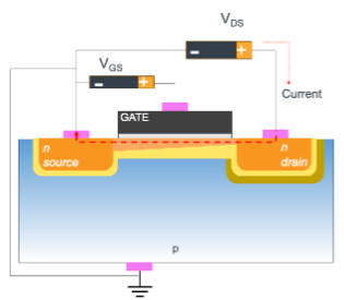
This is an NMOS transistor. As configured, current will flow in the direction shown in red. Electrons will flow in the opposite direction. Increasing Vds will increase the current if the transistor is operating in the Ohmic or linear region. As Vds continues to increase past the Ohmic region, a pinching point in the channel will occur. This is why the channel is more narrow on the drain side than it is on the source side.
All are true regarding IC manufacturing processes:
Deposition and thermal oxidation are additive processes.
CMP and etch are subtractive processes.
“During the IC manufacturing process, circuit elements and structures are made and grown only above the original wafer surface, and into the wafer.”
What is the order?
Electric Arc Furnance: the creation of metallurgical grade silicon
Mining
Chemical Vapor Deposition: the creation of polysilicon
The CZ Process
photoresist and mask move rapidly in the step and scan process.
The pellicle is at the first mask
If this system was an 193i illumination system the BOTTOM of the water that represents the “immersion” or “i” be located on top of the wafer.
pupil filter: is used to control the light exposure to the wafer during lithography, improving resolution and depth of focus.

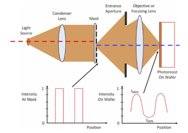
Where is the aerial image?
Is the light intensity on top of the wafer.

Where is the diffraction pattern?
What does “photo” in photoresist mean?
The main idea is we want to create a differential solubility so that part of the pattern is removed during the develop state.
What does “resist” in photoresist mean?
What is the correct description of DNQ-Novolac resist?
That light interacts at the location where the nitrogen (shown by two balls labeled “N”) attaches to the carbon in the aromatic ring structure. This causes the N2 to break off from the DNQ and be released as gas. Water present in the atmosphere attaches to the molecule and ofrms carboxylic acid.
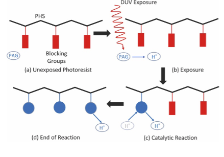
What is the correct description for how a Chemically Amplified Resist system works?
“For a chemically amplified resist (CAR), the “photon doe” occues when the wafer is in the imaging system. The photon
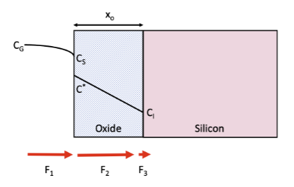
What is the description of the model?
The figure illustrates the Deal-Grove model for the formation of silicon dioxide on top of silicon.