exam 3
 Call Kai
 Learn
Learn Practice Test
 Spaced Repetition
 Match
Match Flashcards
 Knowt Play
1/18

There's no tags or description
Looks like no tags are added yet.
Name | Mastery | Learn | Test | Matching | Spaced | Call with Kai |
|---|
No analytics yet
Send a link to your students to track their progress
19 Terms
What are the levels of packaging?
Level 0 Packaging: Intraconnections on the chip (the internal wiring inside the individual IC die itself).
Level 1 Packaging: Chip to package interconnections to form IC package (e.g., dual in-line package; includes die and wire bonding).
Level 2 Packaging: IC package to circuit board interconnections (soldering the packaged chips onto the PCB).
Level 3 Packaging: Circuit board to rack; card-on-board packaging (plugging multiple circuit boards into a shared rack or backplane).
Level 4 Packaging: Wiring and cabling connections in cabinet (the final system-level cables connecting different racks and power systems inside the main product cabinet).
What is the difference between die bonding and wire bonding?
Die bonding refers to attaching the IC chip (the die) to a package base. The method used varies depending on the material of the package, eutectic d.b. if ceramic (applies thin gold layer on bottom of chip then presses onto a heated package (called eutectic bc they bond due to the eutectic composition of the gold and si hardening together)) and epoxy d.b. (dispenses liquid adhesive (usually epoxy) on chip followed by thermal curing to harden)
Wire bonding refers to creating an electrical connection from the contact pads of the IC chip to the package leads in which that connection is created using aluminum or gold wires to connect the pad and leads.
What are some advantages of SMT? What are some disadvantages/limitations?
Advantages: 1) smaller components and packing density, can mount a lot (so much so that you can use a smaller PCB to achieve the same intended function); 2) can mount on both sides of the PCB; 3) # of drilled holes reduced;
Disadvantages: 1) expensive; 2) harder for people to handle due to the miniature size (harder to do inspection, testing, and rework); 3) some electronic components aren’t available through SMT
How is raw silicon processed to EGS?
1) Take silica sand/quartzite and purify to 98% pure silicon
2) Take 98% Si and mix with HCl to get trichlorosilane (SiHCl3), boil and distill
3) Take SiHCl3 and mix with H2 (hydrogen gas) to get 99.9999999999999% pure Si
Describe the Czochralski process
Motivation: you want the crystal lattice of your wafer structure to be monocrystalline (one direction)
1) Melt EGS to molten silicon in vacuum chamber
2) Dip a seed crystal in the molten Si (seed crystal serves as a perfect crystal template that has a lattice in an aligning single direction)
3) Rotate seed crystal and go upwards, cooling molten Si will mirror the seed crystal and create a uni-directional crystal lattice; boule created
Describe the sequence of the Planar Process
1. Form SiO2 layer on Si wafer: either via Thermal Oxidation using O2 or steam (H2O) (consumes 0.44d of Si, where d is thickness of newly formed SiO2 layer) OR deposit via CVD (Chemical Vapor Deposition) if substrate is not Si. Clean surface to promote wetting/adhesion.
2. Apply liquid photoresist on top by pouring at wafer center then spin coat to distribute evenly on wafer
3. Soft-bake to harden resist at ~90 deg-C for 10-20 min, removing solvents and improving resist adhesion
4. Align mask close to wafer then apply exposure technique (contact, proximity, projection) to transfer UV radiation onto resist
5. Develop photoresist in developer (immersion / spraying) to remove UV exposed areas → rinse and clean to stop development
6. Hard-bake to expel harmful developer components and also increase resist adhesion
7. Etch target layer: Use Wet Etching (HF acid solution, isotropic, causes undercut, high selectivity) to unprotected areas OR Dry Plasma Etching (gas ions to create plasma, anisotropic/directional, no undercut for small features).
8. Remove photoresist w/ wet stripping (liquid chemicals) or dry stripping (plasma etching)
9. Deposit conductive/structural layers: Use CVD to blanket-deposit polysilicon gate or SiO2 over non-Si materials. Use PVD (Sputtering/Evaporation) to deposit metal layers (Al or Cu) for wiring.
10. Introduce impurities (Doping): Shoot Boron (p-type, acceptor) or Arsenic/Phosphorus (n-type, donor) into selected regions via Ion Implantation at room temp.
11. Final Protection: Deposit P-glass layer via CVD to protect completed circuitry from environment
Describe the difference amongst the three different exposure techniques in lithography.
Contact Printing: The photomask is pressed directly against the photoresist. Advantage: Provides very high pattern resolution on the wafer surface; Disadvantage: Direct physical contact gradually wears out and damages the expensive mask.
Proximity Printing: The photomask is slightly separated from the photoresist by a tiny gap (10—25 μm). Advantage: Eliminates physical mask wear and extends its lifespan; Disadvantage: Light diffraction across the gap reduces image resolution.
Projection Printing: High-quality optics project the mask image onto the wafer without touching it (mask in between lens above photoresist), allowing the pattern to be optically reduced for ultra-high resolution. Industry Standard: This is the preferred method due to non-physical contact and high res imaging, which is dominated globally by ASML.
ASML Tech: Modern projection systems use Extreme Ultraviolet (EUV) light inside a total vacuum chamber (since EUV is absorbed by air) using ultra-precise mirrors instead of lenses, because EUV light passes through glass but can be reflected.
What are the many ways to add, alter, or remove layers in IC fab.?
Adding: Thermal Oxidation, CVD, Metallization
Altering: Thermal diffusion, Ion implantation
Removing: Etching
What are some functions of SiO2 in fabrication?
- SiO2 is an insulator, compared to Si which is a semiconductor
- Used as a mask to prevent diffusion or ion implantation of dopants into silicon
- Can be used to isolate devices in circuit
- Provides electrical insulation between levels in multi-level metallization systems
Why would I use metallization? What materials are used in metallization? Processes?
Metallization is used to form conductive patterns on the substrate in IC fab.. It’s great for: 1) forming specific device components on the chip, 2) forming intraconnecting conduction paths, 3) interconnections for chip to ext. circuits
Materials: aluminum historically (good for intraconnections and external interconnections), now copper is more widely used for this purpose; gold, silicides, refractory metals (these last three are good for gates and contacts)
Processes: PVD → vacuum evaporation (ideal for aluminum) and sputtering (aluminum and refractories); CVD → for semiconductor metallization (using silicides and refractories; electroplating → increase thickness of thin films
What is thermal oxidation?
It uses oxygen (O2) or steam (H2O) to oxidize the silicon substrate to form a larger SiO2 layer
0.44d is lost from the Si substrate (d being the thickness of the new SiO2 layer)
What is chemical vapor deposition?
CVD is used when you can’t use thermal oxidation b/c of the non-Si substrate you’re using → still makes an SiO2 layer
Process:
1) SiH4 (silane) + O2 mixes and enters quartz tube w/ pusher gas N2
2) quartz tube is baked to 425 degC
3) Broken down gas molecules from baking rain down to form SiO2 layer
4) Waste exits tube
(To create polysilicon, simple SiH4 reduction baked at 600 degC)
(To create silicon nitride as a masking layer, silane and ammonia (SiH4 + NH3) are mixed and baked at 750 degC)
What are some common doping elements?
Acceptors (p-type): Boron (B)
Donors (n-type): Phosphorus (P), Arsenic (As), Antimony (Sb)
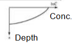
What is thermal diffusion?
It is a doping process where atoms migrate from high to low concentration. It is desired bc it enables controlled doping to reach a desired impurity concentration
Process:
1) Predeposition: deposit dopant gas onto the wafer surface
2) Drive-in: heat treat to redistribute dopant and reach desired depth-concentration profile
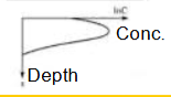
What is ion implantation?
It is a process where an electric field accelerates impurity ions at the Si substrate where they stop (determined by mass and acceleration) at some depth after losing energy
Adv: 1) can be performed at room temp., 2) can use exact doping density (i.e. you have total control over # of atoms accelerated and doped)
What is the difference between wet etching and dry etching?
Wet chemical etching is isotropic, leaves an undercut under the resist, forcing you to design the resist to compensate for this undercut
Dry plasma etching is anisotrophic and etches using plasma from ionized gas (gas mixture enters vacuum and electrical energy creates a plasma from this mix.)
What is the IC Fabrication sequence?
(1) Si3N4 is deposited w/ CVD on Si substrate and patterned (selectively etched using photolithography)
(2) SiO2 is grown by thermal oxidation in unmasked regions
(3) Remove Si3N4 mask
(4) thin layer of SiO2 gate formed by thermal oxidation
(5) polycrystalline silicon (polysilicon) is deposited by CVD and doped n+ using ion implantation
(6) poly-Si pattern etched to define gate electrode
(7) source and drain are formed by doping n+ in Si substrate
(8) P-glass CVD’d onto surface for protection
What are some manufacturing issues that come up in IC packaging?
1) Chip separation (singulation), cutting wafer into individual chips; 2) issues when connecting die to package; 3) chip encapsulation; 4) circuit testing
What materials are used in IC packaging? Adv’s and limitations?
Ceramics (alumina); Adv: hermetic (airtight) sealing, can have complex packages; Disadv: dim control not great b/c package shrinks during formation
Plastic (epoxy, etc.); Adv: low cost,