Electronic Structures of Solids
1/24
There's no tags or description
Looks like no tags are added yet.
Name | Mastery | Learn | Test | Matching | Spaced | Call with Kai |
|---|
No analytics yet
Send a link to your students to track their progress
25 Terms
Give the equation for the Bloch function - what is it used for?
General wavefunction used to describe the crystal orbital:
Ψ( r) = eikr μ( r) → Ψ( r) = N-1/2 Σeikna ΨAO(n) (r-na)
What is the boundary condition for Bloch’s function?
The electronic wavefunction has to have the same value at the beginning and end of the chain hence: kNa = n(2π) (i.e. k is quantised for a finite ring).
N - number of unit cells.
a = length of unit cell.
k = wave vector.
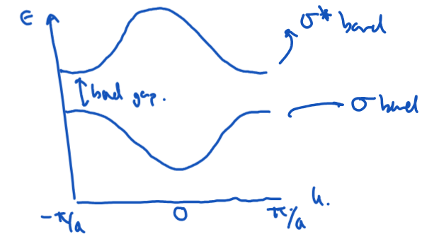
Outline the Brillouin zone (for a 1D chain). How does this arise from the boundary condition?
Due to the periodicity of k, we only need to consider one cell of reciprocal space = first Brillouin zone.
The Brillouin zone = a region of unique electron states (non-repeating k values) that follows from the Bloch boundary conditions.
For a 1D chain, Brillouin zone = -π/a < k< +π/a
What is k for the most bonding and most antibonding cases?
k = 0 → most bonding case
k = π/a → most antibonding case
In a band structure diagram, what does a band represent?
Each band represents the allowed energy of an electron (an atomic orbital) e.g. for H, there is one unit atom per unit cell and one AO per atom → single band. For H2 unit cells → 2 bands (one bonding and one antibonding)
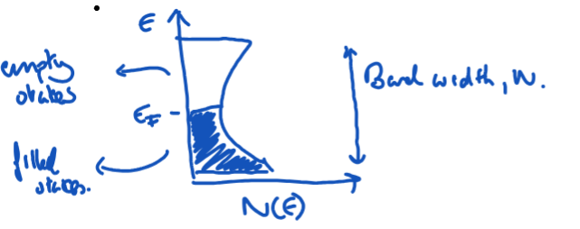
Explain what a DOS plot shows? What does a peak in the DOS plot represent? (draw a basic plot and label)
Vertical axes = energies of electronic states. Horizontal axes = density of states, N(E), which is the number of allowed energy levels per unit volume of the solid.
A peak in the DOS plot indicates a large number of crystal orbitals with similar energies.
EF = Fermi energy
Convert this band structure into a DOS plot.
DOS is large where bands are flat, and small where bands are steep.
At a band minimum or maximum, the DOS shows a peak
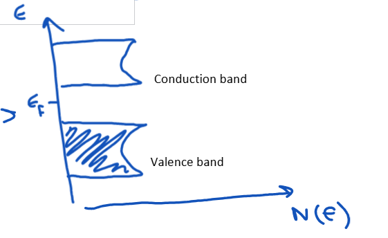
Draw a DOS plot for a metal, semiconductor/insulator and a semimetal.
How is density of states N(E) measured?
Photoelectron spectroscopy - measure KE of the emitted electrons to determine binding energy, which corresponds to the electron’s energy level. The measured intensity at a given binding energy is proportional to the density of states at that energy.
How can we experimentally get information about the band structure?
using angle-resolved PES → momentum of photoelectrons → the component of the wave vector k parallel to the surface.
AR-PES maps E vs k → band structure.
What do bandwidths show about atomic orbitals? How do bandwidths differ for the type or overlap (sigma v pi)?
Bandwidths tell you how 'spread out' an electronic band is in energy. Large bandwidths show strong overlap between atomic orbitals, typical of metals.
Hence core orbital (poor spatial overlap) → narrow bands.
sigma overlap > pi overlap, so sigma bonding bands are wider.
Outline the Fermi-Dirac distribution and state the function
At finite temperatures, thermal energy excites some electrons into states with energies greater than the Fermi energy, creating vacancies in states with energies less than.
f(E) = 1/(1+e(E-EF)/kBT), where f(E) = probability that a given electronic state/crystal orbital is occupied. Note: kBT expressed in units of eV.
Give the equation for conductivity (including both charge carriers)
σ = ne|e|μe + nh|e|μh (electrons and holes)
n = number of mobile charge carriers
μ = mobility
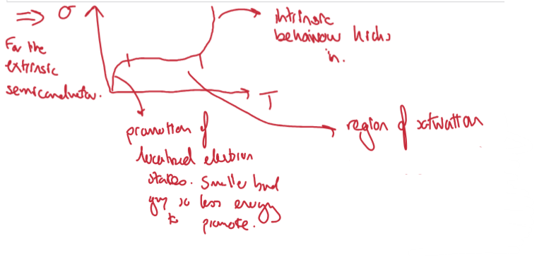
From the Fermi-Dirac distribution/function, explain why metals are better conductors. When does conduction occur?
Conductivity is proportional to the number of mobile charge carriers.
Metals have a large density of states at the Fermi energy and therefore have high conductivity even at low temperatures, I.e. there are many available states near the fermi energy for electrons to occupy and move into.
For insulators / semiconductors, there are very few electrons promoted to the conduction band, hence conductivity is much weaker than metals.
If Eg >> 2kBT then no electrons are promoted and no conduction can occur. At room temperature (298K) this is equal to any value over 0.05 eV.
How does conductivity change with temperature for: 1. metals, 2. intrinsic semiconductors?
Metals: increasing the temperature leads to a very small change in the number of charge carriers and the decreased mobility of the electrons dominates (due to lattice vibrations).
Intrinsic Semiconductor: dramatic increase in the number of charge carriers with temperature.
Define intrinsic vs extrinsic in the context of semiconductors
Intrinsic semiconductors are pure materials with no impurities.
Extrinsic semiconductors are doped with impurities to enhance conductivity.
Extrinsic semiconductors can be classified into two types N-type and P-type.
Draw the basic DOS plot for n type and p type extrinsic semiconductors.
How does the conduction change with temperature for an extrinsic semiconductor?
What are p-n junctions?
when a p-type semiconductor and an n-type semiconductor are brought into contact.
The fermi energy is higher in n-type than p-type to allow electrons to flow from n to p. Electrons and holes cancel out at contact area —> depletion region (insulating barrier between the two semiconductors)
What happens in a p-n junction when a voltage. Give for when V < 0 and when V > 0
V < 0 = reverse bias: Electrons will flow downhill to the n-type (where there is positive charge) and holes move uphill to the p-type.
Band bending at the junction increases.
The depletion zone increases and current flow is reduced.
V > 0 = forward bias. If the polarity of the voltage source is reversed, so that electrons are no longer stable at the n-type.
the band bending at the junction is reduced, and current begins to flow across the junction.
What is the selection rule for semiconductor transitions
Selection rule: Δk = 0 (I.e. when an electron recombines with a hole and emits a photon momentum must be conserved).
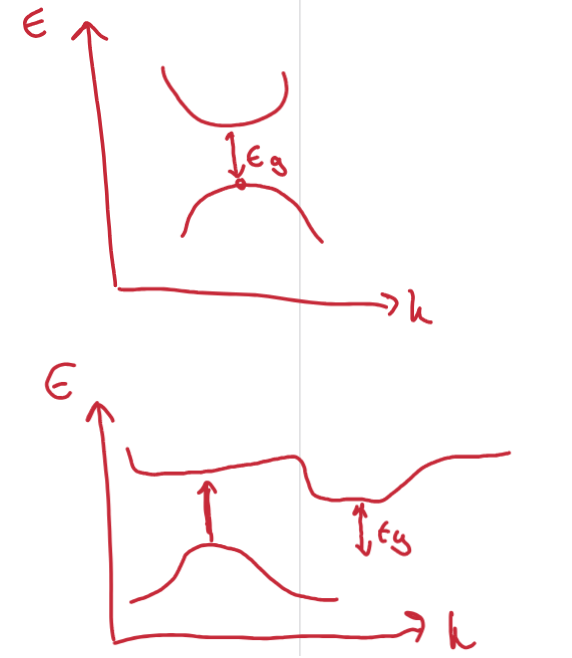
Draw a direct and indirect band gap. Explain their efficiency for light emission
Direct: max and minima align. Electron-hole pair recombination can occur through a Δk = 0 transition, emitting a photon (luminescence).
Indirect: Where the distance vertically in the band structure is greater than the band gap. No pure photon emission loss processes available – when an electron transitions from the valence band to the conduction band, it must change its momentum. This makes indirect band gap materials less efficient for light emission. Can view the promoted electron as 'trapped' in the conduction band.
What are the requirements for a good solar cell?
must have a band gap of less than 1.8 eV (absorb over the entire visible range).
direct band gap.
many use p-n junctions (
Why are most metals not coloured? Give some exceptions
there are plenty of suitable transitions that meet Δk = 0 for them to absorb across the whole visible spectrum.
Au and Cu are coloured – there are s-like bands near the Fermi level above d bands. No optical Δk = 0 transitions are available from the s band near the Fermi level upwards. Instead start below the Fermi level and excite to the unfilled part of the s-bands.
Draw the diagram/explain how an LED works - what is required for an efficient LED?
LED emits light under forward bias: electrons within the n-type conduction band move towards the p-type conduction band. The electrons then drop to the valence band, and a photon is emitted during electron-hole recombination. Requires a direct band gap/