Electronic Devices Lectures
 Note
Note Call Kai
 Learn
Learn Practice Test
 Spaced Repetition
 Match
Match Flashcards
 Knowt Play
1/80

There's no tags or description
Looks like no tags are added yet.
Name | Mastery | Learn | Test | Matching | Spaced | Call with Kai | Chat |
|---|
No analytics yet
Send a link to your students to track their progress
81 Terms
how does f(E) depend on temperature?
it gradually increases as temperature increases.
what is the occupancy of a state at E = Ef?
50%
what is the fermi energy of fermi level Ef?
the eneryg where seeing an electron is 50%
how does density of states g(E) depend on energy E?
Regardless of E, g(E) stays the same. no dependancy
which groups form semiconductors?
II, III, IV, V, VI. ie (1-6_
miller index direction syntax
[]
miller index surface syntax
()
wafer thickness or chip size
mils (10e-3 inches = 25.4 micrometers)
ni of silicon
1×10^10 / cm³
crystalline silicon band electrons
not tied to or associated with any one particular atom
forbidden zone
a crystal containing only Si atoms with no impurities gives rise to the conduction and valence bands with no levels in the band gap
what are the n values for shell k, shell L, shell m, shell n,
1 , 2, 3, 4
Ideal Component
A component that takes no space, weighs nothing, uses no power, costs nothing, requires no maintenance, no training to operate, and lasts forever.
“Smart weightless power costs more training but lasts forever.”
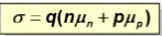
Conductivity Equation
Describes the relationship between resistance, current, electron charge, number of free electrons, and holes in a semiconductor.
o Q = 1.602 * 10-19 (c) = Electron charge
o N – number of free electrons (e-)
o P – number of free holes (h+)
o Mn - how fast the e- is moving
o Mp – how fast the h+ is moving
Semiconductor Types
Classification into elemental and compound semiconductors, focusing on Si, Ge, Ga, As, and their applications.
Crystal Growth
The process of making semiconductors, including crystal structure, wafer slicing, and different lattice types.
Energy Levels, Bonds, and Bands
Concepts related to electronic atom structure, energy bands, covalent bonds, and carriers in semiconductors.
Fermi Function f(E)
Gives the probability of a state being occupied by an electron, influencing the behavior of electrons in a semiconductor crystal.
Density of States g(E)
The number of available states for electrons in a semiconductor, crucial for understanding electron occupancy and behavior.
an si atom has how many electrons
14
how many atoms are there in the three dimensional diamond lattice unit cell?
8
Bell Labs (1947)
the 1st transistor was made.
o John Bardeen
o Walter Brattain
o William Shockley
device dimensions
o Microns (micrometers) – 10-6
·Oxide thickness
o Angdstroms (A) or nanometers (nm) – 10-9
wafer diameters
o Millimeters(mm) or inches
conductivity is determined by the number of __ and __.
electrons and holes
resistivity is the inverse of _______
conductivity
Elemental
using one material
Compound
uses more than one material
semiconductor - group IV
silicon is the most common
in most integrated circuits and power devices
semiconductor- group III and V
GeAs is most common
light emitting - GaN, GaAsP
optical communication - GaLnAsp
semiconductor - group II and VI
lightning arresters - ZnO
Infrared detectors - HgCdTe
how to make a semiconductor
o Bring single crystal seed into the melt
o Dip seed into melt and withdraw slowly
o Pull seed with proper pull rate and rotation
for slicing wafers, what is used?
a wire coated in diamond splinters
1 cpu = _____ mm²
506
Crystals structure - amorphous
§ Randomly distributed, working like an insulator (glass)
Crystals structure - Polycrystalline
Metal, some organization, working like an conductor (most metals)
Crystals structure - single crystal
very organized - semi-conductor - (silicone wafer)
simple cubic lattice
atoms on every corner totaling 1 atom
body centered cubic (bcc)
atoms on every corner AND 1 in the middle totaling 2 atoms
face centered (fcc)
atoms on every corner AND 1 atom on the surface of each face of the cube totaling 4 atoms.
diamond lattice
fcc with 4 additional atoms in the box totaling 8 atoms.
unit cell
small portion of any crystal that could be used to reproduce the crystal
doesnt have to be primitive, the smallest unit cell possible
miller indices
numbers that specify the wafer surfaces
find x, y and z
inverse them
normalize the lowest integers
zincblende structure
same as a diamond lattice EXCEPT there are two different types of atoms in the lattice
GaAs, InP, GaP,
miller indices cannot be established for a plane passing through the ____.
orgin
isolated atom
an atomic core or nucleus surrounded by electrons
principle quantum numbers (n)
determines the energy of an election
Azimuthal quantum number (l)
determines the angular momentum magnitude.
each value of l constitutes a subshell
conduction band (Ec)
higher band, can hold 8 electrons
band gap (Eg)
amount of energy gained or lost by the charge of a single electron moved across an electric potential different of 1 volt
electrons cannot exist in this gap
determines the characteristics of the device (ie. metal, semiconductor, insulator)
what is the band gap (Eg) of silicone?
1.12 eV
lower band gap energy = lower _________ = higher ______________
resistance, conductivity
at low temperatures, there are no electrons in the ____________ band and no holes in the ____________ band. aka..there is no current.
conduction, valence
free electrons
only in the conduction band
free holes
only in the valence band
current equation
i = dQ/Dt
Q = charge = free electrons and free holes
electron hole pair (EHP)
for every free hole there is a free electron
dopant atoms
specific impurities added to semiconductors
donor atom
group V atoms (P, As, Sb)
Extra electron
At higher temps, donor donates extra electron
n - type (electrons are majority carrier)
Acceptor atom
group III atoms (B, Ga, In)
missing an electron
at higher temps, acceptor takes an electron
P-type
intrinsic semiconductor
undoped semiconductor sample containing any significant amount of impurity atom
number of electrons (n) = number of holes(i) = ni
ni for si = 1×10^10 cm³
extrinsic semicondcutor
doped semiconductor
majority carrier
the most abundant carrier in a given semiconductor sample
electrons in an n-type material
minority carrier
the least abundant carrier in a given semiconductor sample
holes in an n-type material
density of states
number of chairs available for electrons
effective mass (Mn*)
mass of electrons in a crystal. different from the mass of electrons in the free space
fermi function f(E)
gives the probability of a state being occupied by an election
fermi energy Ef
where the probability of seeing an electron is 50%. going up decreased the probability but going down increases the probability
boltzmann constant (k)
8.617 × 10^(-5)
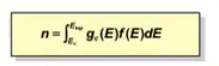
electron density
depends on the area under the (E - Ec) vs gc(e) curve
what material parameters determine the semiconductor resistivity?
carrier density (electron and hole) and mobility
which one material parameter influence the semiconductor resistivity the most?
dopant density
what shell do si atoms have 4 electrons in?
M shell
charge of electron
1.6 × 10^-19 C
how many atoms are there in the (100) plane?
2