14. Semiconductor Electronics: Materials, Devices and Simple Circuits
 Call Kai
 Learn
 Practice Test
 Spaced Repetition
 Match
 Flashcards
 Knowt Play
1/99

Earn XP
Description and Tags
Theory/formula revision for Semiconductors. Question mode: Flashcards only. Answer mode: Answer with Definition. Recommended Study mode: Spaced Repetition. This set is based purely on the NCERT chapter, and is suitable for revision for IAT, NEET. Some material from JEE is missing. Good luck with exams!!
100 Terms
In a vacuum tube, the electrons are supplied by which electrode when heated?
Cathode.
Why are vacuums required in vacuum tubes?
Vacuum is required in the inter-electrode space; otherwise the moving electrons may lose their energy on collision with the air molecules in their path.
In vacuum tubes, which direction do electrons flow in? (relative to electrodes)
Electrons flow from cathode to anode.
Why are vacuum tubes also called valves?
In these devices the electrons can flow only from the cathode to the anode (i.e., only in one direction). Therefore, such devices are generally referred to as valves.
Why are vacuum tubes unreliable?
Vacuum tube devices are bulky, consume high power, operate generally at high voltages (~100 V) and have limited life and low reliability.
Why are solid state semiconductor electronics more reliable?
No external heating or large evacuated space is required by the semiconductor devices. They are small in size, consume low power, operate at low voltages and have long life and high reliability.
Much before the full implications of the semiconductor devices was formally understood, a naturally occurring crystal of ____________________ with a metal point contact attached to it was used as detector of radio waves.
Much before the full implications of the semiconductor devices was formally understood, a naturally occurring crystal of galena (Lead sulphide, PbS) with a metal point contact attached to it was used as detector of radio waves.
What is the range of values of conductivity and resistivity in metals?

What is the range of values of conductivity and resistivity in semiconductors?

What is the range of values of conductivity and resistivity in insulators?

What are two examples of elemental (intrinsic) semiconductors?
Si and Ge
What are two examples of inorganic compound semiconductors?
CdS and GaAs
What are two examples of organic compound semiconductors?
Anthracene, doped pthalocyanines
What are three examples of organic polymer semiconductors?
polypyrrole, polyaniline, polythiophene, etc.
What are energy bands inside solids?
Inside the crystal each electron has a unique position and no two electrons see exactly the same pattern of surrounding charges. Because of this, each electron will have a different energy level. These different energy levels with continuous energy variation form what are called energy bands.
What is the valence band and conduction band?
The energy band which includes the energy levels of the valence electrons is called the valence band. The energy band above the valence band is called the conduction band.
What is the distribution of electrons in the valence band and conduction band in conductors with no external energy?
If the lowest level in the conduction band happens to be lower than the highest level of the valence band, the electrons from the valence band can easily move into the conduction band. Normally the conduction band is empty. But when it overlaps on the valence band electrons can move freely into it. This is the case with metallic conductors.
What is the distribution of electrons in the valence band and conduction band in insulators with no external energy?
With no external energy, all the valence electrons will reside in the valence band.

What sort of material has this energy band structure?
conductors

What sort of material has this energy band structure?
conductors

What sort of material has this energy band structure?
insulators

What sort of material has these sort of energy bands?
semiconductors
What is the range of values that the energy band gap can be in semiconductors?
0.1eV to 3eV
In intrinsic semiconductors, what is the relationship between the number of free electrons and the number of holes?
In intrinsic semiconductors, the number of free electrons, ne is equal to the number of holes, nh. That is:
ne=nh=ni
What is intrinsic carrier concentration (ni)?
ne=nh=ni
where:
ne is the number of free electrons in an intrinsic semiconductor
nh is the number of holes in an intrinsic semiconductor
In doped semiconductors, this relation looks like:
nenh=ni2
What is the total current inside a semiconductor with respect to the movement of electrons and holes inside it?
The total current, I is thus the sum of the electron current Ie and the hole current Ih:
I=Ie+Ih
What is the “process of generation” and “process of recombination”?
Process of generation: electrons enter the conduction band, leaving behind holes, increasing carrier concentration.
Process of recombination: conduction electrons recombine with the holes by colliding into them, decreasing carrier concentration.
What is equilibrium in terms of the process of generation and recombination?
At equilibrium, the rate of generation is equal to the rate of recombination of charge carriers.
An intrinsic semiconductor at 0 K will act like ____________.
(conductor, insulator)
An intrinsic semiconductor at 0 K will act like an insulator.
C, Si and Ge have same lattice structure. Why is C insulator while Si and Ge intrinsic semiconductors?
[DIRECTLY FROM NCERT]
The 4 bonding electrons of C, Si or Ge lie, respectively, in the second, third and fourth orbit. Hence, energy required to take out an electron from these atoms (i.e., ionisation energy Eg) will be least for Ge, followed by Si and highest for C. Hence, number of free electrons for conduction in Ge and Si are significant but negligibly small for C.
[DIRECTLY FROM NCERT]
What is an extrinsic semiconductor?
When a small amount, say, a few parts per million (ppm), of a suitable impurity is added to the pure semiconductor, the conductivity of the semiconductor is increased manifold. Such materials are known as extrinsic semiconductors or impurity semiconductors or doped semiconductors.
What is doping? What are dopants?
The deliberate addition of a desirable impurity in an intrinsic semiconductor is called doping and the impurity atoms are called dopants.
Why is it important for sizes of dopant atoms to be similar to the size of semiconductor atoms?
The dopant has to be such that it does not distort the original pure semiconductor lattice. It occupies only a very few of the original semiconductor atom sites in the crystal. A necessary condition to attain this is that the sizes of the dopant and the semiconductor atoms should be nearly the same.
State 3 examples of pentavalent dopants.
Arsenic (As), Antimony (Sb), Phosphorus (P)
State 3 examples of trivalent dopants.
Indium (In), Boron (B), Aluminium (Al)
Which type of dopant is used to create n-type semiconductors?
pentavalent dopants.
Which type of dopant is used to create p-type semiconductors?
trivalent dopants.
What are the majority carriers in n-type semiconductors?
electrons
What are the majority carriers in p-type semiconductors?
holes
What is the ionisation energy required in doped Ge and Si, as well as pure Ge and Si, to start conducting?
In doped semiconductors, the energy required is 0.01eV for germanium, and 0.05eV for silicon, to separate this electron from its atom. This is in contrast to the energy required to jump the forbidden band (about 0.72eV for germanium and about 1.1eV for silicon) at room temperature in the intrinsic semiconductor.
[it’s probably not required to remember precise values, but remember the general trend]
Which sort of dopant is known as a “donor impurity”? What does it donate?
pentavalent dopant, as it donates an electron
In n-type semiconductors, the number of electrons made available for conduction by dopant atoms depends on what factors?
The number of electrons made available for conduction by dopant atoms depends strongly upon the doping level and is independent of any increase in ambient temperature.
In n-type semiconductors, the number of electrons made available for conduction by semiconductor atoms depends on what factors?
The number of free electrons (with an equal number of holes) generated by Si/Ge atoms, increases weakly with temperature.
What is the relationship between ne and nh in n-type semiconductors?
ne>>nh
Which sort of dopant is known as “acceptor impurity”? What does it accept?
trivalent dopant, as it accepts electrons.
The dopant atom of ________ material can be treated as core of one negative charge.
(n-type, p-type)
The dopant atom of p-type material can be treated as core of one negative charge.
What is the relationship between ne and nh in p-type semiconductors?
nh>>ne
When dopants are added to semiconductor crystals, the impurity creates additional electrons/holes for conduction. Therefore, they change the overall charge on the semiconductor. True or false?
False.
The crystal maintains an overall charge neutrality as the charge of additional charge carriers is just equal and opposite to that of the ionised cores in the lattice.
How do majority carriers in doped semiconductors reduce the intrinsic concentration of minority carriers?
In extrinsic semiconductors, because of the abundance of majority current carriers, the minority carriers produced thermally have more chance of meeting majority carriers and thus getting destroyed. Hence, the dopant, by adding a large number of current carriers of one type, which become the majority carriers, indirectly helps to reduce the intrinsic concentration of minority carriers.
How is a semiconductor’s energy band structure affected by doping?
In the case of extrinsic semiconductors, additional energy states due to donor impurities (ED) and acceptor impurities (EA) also exist.
What are the changes to a doped semiconductor’s energy band structure in the case of n-type semiconductors?
In the energy band diagram of n-type Si semiconductor, the donor energy level ED is slightly below the bottom EC of the conduction band and electrons from this level move into the conduction band with very small supply of energy.
What are the changes to a doped semiconductor’s energy band structure in the case of p-type semiconductors?
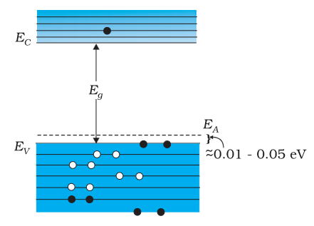
The acceptor energy level EA is slightly above the top EV of the valence band. With very small supply of energy an electron from the valence band can jump to the level EA and ionise the acceptor negatively.
Alternately, we can also say that with very small supply of energy the hole from level EA sinks down into the valence band.
The electron and hole concentration in a semiconductor (doped or otherwise) in thermal equilibrium is given by which relation?
nenh=ni2
where:
ne is the number of free electrons
nh is the number of holes
ni is the intrinsic carrier concentration
What are the intrinsic energy gap values for Carbon, Silicon, and Germanium?
For C (diamond), Si and Ge, the energy gaps are 5.4eV, 1.1eV and 0.7eV, respectively.
[It’s probably not necessary to remember exact values, but remember that for C it is greater than 3eV, different from Si and Ge.]
What sort of semiconductor has this energy band structure?
p-type semiconductor at T>0K
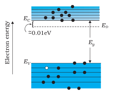
What sort of semiconductor has this energy band structure?
n-type semiconductor at T>0K
What are the two important processes in relation to carriers that take place at a p-n junction?
diffusion and drift
Which carrier movement gives rise to the diffusion current across a p-n junction?
Due to the concentration gradient across p-, and n- sides of the semiconductor (electrons being a majority in the n-side and holes being a majority at the p-side), holes diffuse from p-side to n-side (p → n) and electrons diffuse from n-side to p-side (n → p). This motion of charge carries gives rise to diffusion current across the junction.
What is a depletion region in a semiconductor?
The space-charge region on either side of the junction together is known as depletion region as the electrons and holes taking part in the initial movement across the junction depleted the region of its free charges.
Which carrier movement gives rise to the drift current across a p-n junction?
Due to this the electric field generated across a depletion region, an electron on p-side of the junction moves to n-side and a hole on n-side of the junction moves to p-side. The motion of charge carriers due to the electric field is called drift. Thus, a drift current starts.
The drift current is in the opposite direction to the diffusion current in a semiconductor. True or false?
True.
How is equilibrium reached between a diffusion current and a drift current in a semiconductor?
Initially, diffusion current is large and drift current is small. As the diffusion process continues, the space-charge regions on either side of the junction extend, thus increasing the electric field strength and hence drift current. This process continues until the diffusion current equals the drift current. Thus a p-n junction is formed. In a p-n junction under equilibrium there is no net current.
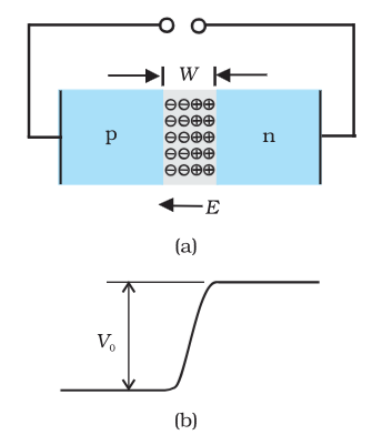
What is V0 here?
Barrier potential
What is barrier potential across a p-n junction?
The loss of electrons from the n-region and the gain of electron by the p-region of the semiconductor (across the p-n junction) causes a difference of potential across the junction of the two regions. The polarity of this potential is such as to oppose further flow of carriers so that a condition of equilibrium exists. Since this potential tends to prevent the movement of electrons from the n region into the p region, it is often called a barrier potential.
Can we take one slab of p-type semiconductor and physically join it to another n-type semiconductor to get p-n junction?
[DIRECTLY FROM NCERT]
No! Any slab, howsoever flat, will have roughness much larger than the inter-atomic crystal spacing (~2 to 3 Å) and hence continuous contact at the atomic level will not be possible. The junction will behave as a discontinuity for the flowing charge carriers.
[DIRECTLY FROM NCERT]

What is the circuit symbol for this electronic component?


In which direction does the conventional current flow across this component when it is in forward bias?
From p to n.
Under forward bias, which terminals are connected to the p-side and n-side of a semiconductor diode?
p-side is connected to the positive terminal of the battery and n-side to the negative terminal.
The applied voltage under forward bias mostly drops across the depletion region of a semiconductor diode and the voltage drop across the p-side and n-side of the junction is negligible.
Why?
This is because the resistance of the depletion region – a region where there are no charges – is very high compared to the resistance of n-side and p-side.
Under _______ bias, the direction of the applied voltage (V) is opposite to the built-in potential V0.
(forward, reverse)
Under forward bias, the direction of the applied voltage (V) is opposite to the built-in potential V0.
What is the expression for the effective barrier height of a semiconductor diode under forward bias?
V0−V
where:
V0 is the barrier potential of the semiconductor diode
V is the applied voltage
What is minority carrier injection in semiconductors?
Due to the applied voltage under forward bias, electrons from n-side cross the depletion region and reach p-side (where they are minority carries). Similarly, holes from p-side cross the junction and reach the n-side (where they are minority carries). This process under forward bias is known as minority carrier injection.
What is the major contributor to forward current across a diode under forward bias? What is the minor contributor?
At the junction boundary, on each side, the minority carrier concentration increases significantly compared to the locations far from the junction, due to minority carrier injection.
Due to this concentration gradient, the injected electrons on p-side diffuse from the junction edge of p-side to the other end of p-side. Likewise, the injected holes on n-side diffuse from the junction edge of n-side to the other end of n-side. This motion of charged carriers on either side gives rise to current. The total diode forward current is sum of hole diffusion current and conventional current due to electron diffusion. The magnitude of this current is usually in mA.
The drift current is also there under forward bias but it is negligible (mA) when compared with current due to injected carriers.
Under reverse bias, which terminals are connected to the p-side and n-side of a semiconductor diode?
n-side is connected to the positive terminal of the battery and p-side to the negative terminal.
What is the expression for the effective barrier height of a semiconductor diode under reverse bias?
V0+V
where:
V0 is the barrier potential of the semiconductor diode
V is the applied voltage
What is the major contributor to forward current across a diode under reverse bias?
The electric field direction of the junction is such that if electrons on p-side or holes on n-side in their random motion come close to the junction, they will be swept to its majority zone. This drift of carriers gives rise to current. The drift current is of the order of a few μA.
The diode ________ current is dependent on applied voltage.
(forward, reverse)
The diode forward current is dependent on applied voltage.
(The reverse current is not very dependent)
The diode _________ current is dependent on concentration of minority carriers on either side of the junction.
(forward, reverse)
The diode reverse current is dependent on concentration of minority carriers on either side of the junction.
What is the breakdown voltage of a diode?
The current under reverse bias is essentially voltage independent up to a critical reverse bias voltage, known as breakdown voltage (Vbr). When V=Vbr, the diode reverse current increases sharply. Even a slight increase in the bias voltage causes large change in the current.

The diode in this circuit is under _________ bias.
(forward, reverse)
The diode in this circuit is under forward bias.

The diode in this circuit is under __________ bias.
(forward, reverse)
The diode in this circuit is under reverse bias.
What does the IV characteristic of a typical semiconductor diode look like?

What is the threshold voltage for a semiconductor diode?
In forward bias, the current first increases very slowly, almost negligibly, till the voltage across the diode crosses a certain value. After this characteristic voltage, the diode current increases significantly (exponentially), even for a very small increase in the diode bias voltage. This voltage is called the threshold voltage or cut-in voltage.
What is the value for threshold voltage silicon diode?
~ 0.7 V
What is the value for threshold voltage of a germanium diode?
~ 0.2 V
What is reverse saturation current in a diode?
For the diode in reverse bias, the current is very small (~μA) and almost remains constant with change in bias. It is called reverse saturation current.
What is the formula for dynamic resistance of a diode?
rd=ΔIΔV
where:
rd is the dynamic resistance
ΔV is the small change in applied voltage
ΔI is the small change in current generated

What is the resistance of the diode at −10V applied voltage?
rd=−1μA−10V=1.0×10⁷
What is the circuit for a half-wave rectifier?

What are the input and output voltage waveforms for a half-wave rectifier?

What is the circuit for a full-wave rectifier involving a centre-tap transformer and 2 diodes?

What are the input and output voltage waveforms for a full-wave rectifier without a filter?

What are the two simple methods to obtain a steady DC output from a pulsating voltage from a full-wave rectifier?
To get steady DC output from the pulsating voltage normally a capacitor is connected across the output terminals (parallel to the load RL). One can also use an inductor in series with RL for the same purpose.
What are voltage filters?
To get steady DC output from the pulsating voltage normally a capacitor is connected across the output terminals (parallel to the load RL). One can also use an inductor in series with RL for the same purpose.
Since these additional circuits appear to filter out the AC ripple and give a pure DC voltage, they are called filters.
Capacitor input filters use _______ capacitors.
(large, small)
Capacitor input filters use large capacitors.
Capacitor input filters use large capacitors. Why?
The rate of fall of the voltage across the capacitor depends inversely upon the product of capacitance C and the effective resistance RL used in the circuit and is called the time constant. To make the time constant large, the value of C should be large.
What is the circuit diagram of a full-wave rectifier using a capacitor as a filter?
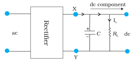
What are the input and output voltage waveforms of a full-wave rectifier with a capacitor as a filter?

How can junction barrier potentials be changed?
By changing the externally applied voltage.
In elemental semiconductors (Si or Ge), the n-type or p-type semiconductors are obtained by introducing ‘dopants’ as defects. What other method is there to obtain different types of semiconductors in compound semiconductors?
In compound semiconductors, the change in relative stoichiometric ratio can also change the type of semiconductor. For example, in ideal GaAs the ratio of Ga:As is 1:1 but in Ga-rich or As-rich GaAs it could respectively be Ga1.1 As0.9 or Ga0.9 As1.1. In general, the presence of defects control the properties of semiconductors in many ways.