EET2210 Final (Ch 5 - 12 review)
1/56
Earn XP
Description and Tags
Name | Mastery | Learn | Test | Matching | Spaced | Call with Kai |
|---|
No analytics yet
Send a link to your students to track their progress
57 Terms
|
Figure A
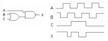
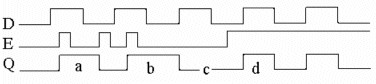
True or False: The waveforms are correct for the logic circuit shown.
False
True or false: adders with greater bit capacities can be constructed by connecting 2-bit adders in parallel.
True
How many gates, including inverters, are required to implement the equation X= A + AB + A’B after it is simplified using Boolean algebra?
1
True or false: converting a decimal number to its binary equivalent is an example of encoding.
True
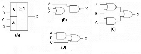
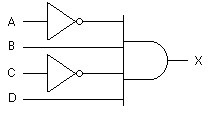
Which circuit in Figure 5-3 represents the NAND implementation of an inverter?
Figure C
True or false: a half-adder has no carry-in bit.
True
Which of the following is true for IC comparator circuits?
All comparators have outputs for indicating A<B, A>B, and A=B.
Comparators can compare only 2 bits at a time.
Comparators can compare only two values at a time.
None of these
Comparators can compare only two values at a time
The symbol in Figure 6-2 represents a(n) ________.
full-adder
The output of the decoder in Figure 6-3 will be 1 only when ________.
A = 0, B = 1, C= 0, D = 1
A multiplexer with four select, or address, lines can select one of ________ inputs.
16
The symbol most likely represents a ________.
multiplexer
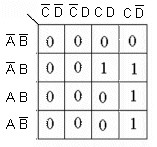
True or false: the Karnaugh map represents the expression, X = ACD + AB(CD + BC).
False
True or false: in binary addition, 1 + 1 = 10.
True
The expression A ⊕ B represents ________.
the sum output of a half-adder
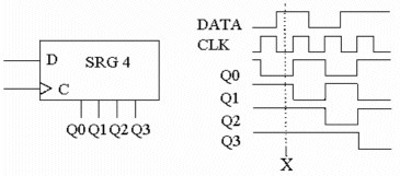
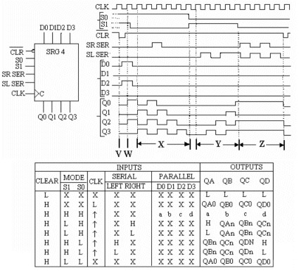
Refer to the circuit and waveforms in Figure 8-2. What value is stored in the register at time 'X'?
1 1 1 0
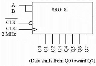
A serial data path needs a 2000 ns delay. Which output from the circuit below will provide the correct delay?
Q3
Refer to Figure 8-5. What occurs at point 'V' on the timing diagram?
The outputs are cleared — set to LOW.
An active-HIGH input S-R latch has a 1 on the S input and a 0 on the R input. What state is the latch in?
Q = 1, NOTQ = 0
Which of the following best describes the action of pulse-triggered flip-flops?
The clock and R-S inputs must be pulse shaped.
A pulse on the clock transfers data from input to output.
The synchronous inputs must be pulsed.
The data is entered on the leading edge of the clock, and transferred out on the trailing edge of the clock.
The data is entered on the leading edge of the clock, and transferred out on the trailing edge of the clock.
Which of the following describes the operation of a positive edge-triggered D flip-flop?
The output will follow the input on the leading edge of the clock.
The input is toggled into the flip-flop on the leading edge of the clock and is passed to the output on the trailing edge of the clock.
If both inputs are high, the output will toggle.
When both inputs are low, an invalid state will exist.
The output will follow the input on the leading edge of the clock.
An astable multivibrator is a circuit that ________.
has two stable states
has one stable state
produces a continuous output signal
Both B and C are correct.
produces a continuous output signal
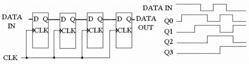
After the DATA IN waveform in Figure 8-1 is complete, what value is stored in the register?
1 1 0 1
What does UART stand for, and what does it do?
United Artists Radio and Television; the standard data interfacing system first used by the movie industry.
Universal ASCII Receiver Transmitter; it is used to transmit and receive ASCII characters.
Universal ASCII Relay Transmission; defines a method (standard) by which data communications can be made between parallel and serial devices or systems.
Universal Asynchronous Receiver Transmitter; it is used to interface the parallel data bus in a typical computer system to serial data transmission lines.
Universal Asynchronous Receiver Transmitter; it is used to interface the parallel data bus in a typical computer system to serial data transmission lines.
Flip-flops are normally used for all of the following applications, except ________.
data storage
logic gates
frequency division
counting
logic gates
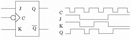
The waveforms for this J-K flip-flop indicate the circuit is operating properly.
False
These waveforms are applied to a gated D latch, which is initially RESET. Which of the areas identified on the Q waveform is incorrect?
Area C
What is the primary function of a register?
Data storage (memory)
Encoding
Counting
Decoding
Data storage (memory)
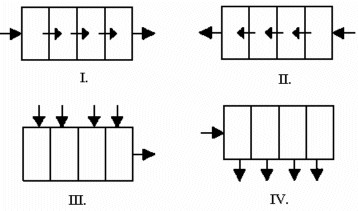
Which of the illustrations below represents the function of a parallel-in serial-out register?
Figure III
What symbol is used to identify edge-triggered flip-flops?
A triangle on the Clock input
Modulus refers to ________.
the maximum number of states in a counter sequence
The remote servers in a cloud storage system are referred to as ________.
nodes
The main difference between a PAL and a GAL is ________.
a GAL uses EECMOS technology and is re-programmable
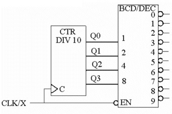
The 'X' in the CLK/X input in Figure 9-10 is normally called the ________, and, in this example, is an active ________ level.
STROBE, LOW
Which Boolean Expressions are implemented by a PAL?
Sum-of-Product
A PAL has a programmable AND array and a programmable OR array.
False
The circuit in Figure 9-11 is used for ________ and for the inputs shown, the DATA OUT will be ________.
parallel-to-serial conversion, 0
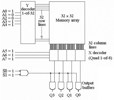
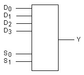
For the circuit of Figure 11-3, how many bits are contained in the output data word?
4
Which of the following is not a type of memory?
FPROM
EEPROMS can be electrically erased and reused.
True
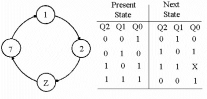
Refer to Figure 9-8. What value should 'X' represent in the state table?
1
When a PAL is programmed, small fuses are blown open to allow connections between the input pins and the AND array.
True
An FPGA (Field Programmable Gate Array) basically consists of an array of logic blocks with programmable row and column interconnecting channels surrounded by programmable I/O blocks.
True
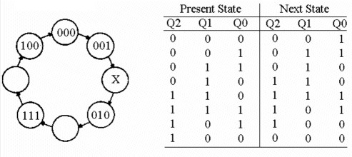
If the diagram shown in Figure 9-6 represents a three-bit Gray code counter, what binary value would exist at 'X'?
011
What is the resolution, in percent, of a 12-bit DAC?
0.024
How do you find the resolution, in percent, of a DAC?
(1 / (2^n) -1) * 100
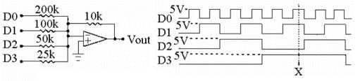
The circuit shown in Figure 12-1 is a(n) ________.
binary-weighted-input DAC
The basic approach to testing D/A converters is to ________.
apply a sequence of binary codes covering the full range of the input to the input while observing the output on an oscilloscope. The output should consist of a linear stairstep ramp
True or false: a digital-to-analog (D/A) converter changes data like temperature variations into digital quantities.
False
What is the accuracy of a D/A converter?
It is the comparison between the actual output of the converter and its expected output.
True or false: the process preformed by an ADC is called quantization.
True
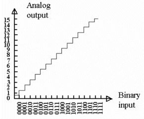
Refer to Figure 12-2. What, if anything, appears to be wrong with the D/A converter?
There is an offset error.
What advantage does the R/2R ladder DAC have over a binary-weighted-input DAC?
It uses only two different resistor values.
An analog quantity varies from 0-7 V and is input to a 6-bit A/D converter. What analog value is represented by each step on the digital output?
0.111 V
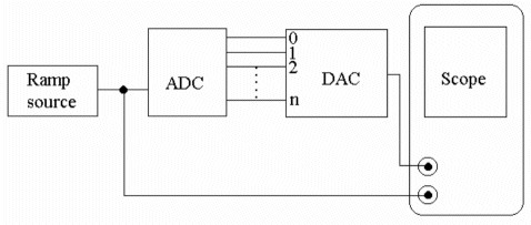
Refer to the figure below. What should the display on the scope look like if the A/D converter is working properly?
A uniform stairstep pattern should be displayed.