Physics Feud 2
1/154
There's no tags or description
Looks like no tags are added yet.
Name | Mastery | Learn | Test | Matching | Spaced | Call with Kai |
|---|
No analytics yet
Send a link to your students to track their progress
155 Terms
Direct semiconductor
Conduction band minimum and valence band maximum are at the same location in k-space
indirect semiconductor
Conduction band minimum and valence band maximum are at different locations in k-space
Photoexcitation of electrons
A photon with an energy greater than Eg can excite can electron from the VB to the CB.
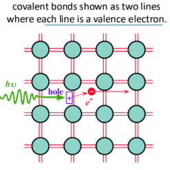
When a photon breaks a Si-Si bond, a free electron and a hole in the Si-Si bond are created.
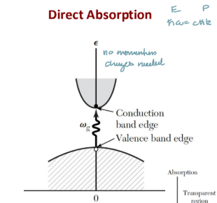
Direct Photon Absorption
absorption of photon which excites electrons from valence band to
conduction band and generates electron-hole pairs
photon energy is same as band gap
No change in momentum (kphoton = Δk ≈ 0)
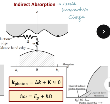
Indirect Absorption
absorption of photon assisted by absorption/emission of phonon that excites electrons from valence band to conduction band and generates electron-hole pairs – satisfying momentum and energy conservation laws.
has to have phonon for conservation of momentum
Thermal generation of electron hole pairs
atoms are constantly vibration above 0 K
Some of the thermal vibrations of atoms may break bonds, thus create electron-hole pairs
Hole
corresponds to empty valence band wavefunction
collective motion of all other electrons
effective positive charge
move due thermal energy activation
Recombination
Hole in valence band meets electron in conduction band and electron fills hole site
excess energy may be released as photon or lost as lattice vibrations
What happens to the system energy as a hole moves downward?
The energy increases
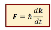
General formula for force on a crystal
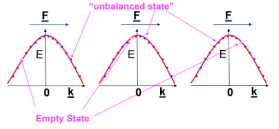
How can electron motion be interpreted as hole motion?
An unbalanced electron moving left is equivalent to a hole moving right
Expression for effective electron mass
The effect of lattice-lattice interactions are wrapped into into ∇kε(k), so now apart of the effective mass
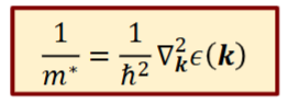
What does a thinner band parabola represent?
A smaller effective electron mass
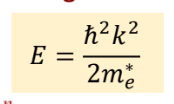
Energy expression using semiconductors
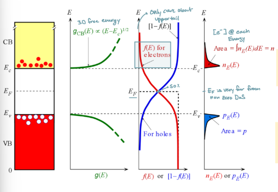
What statistics do we use for semiconductors
Boltzmann, electrons act like classical particles in semiconductors
Why can we assume electrons in a semiconductor behave classically?
non zero energy in the DoS (conduction band and valence band) is very far from fermi level, so the fermi dirac distribution can be approximated by boltzmann stats
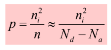
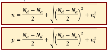
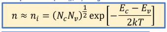
Electron concentration in conduction band formula (intrinsic)
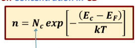
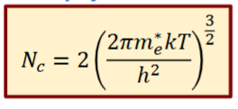
Effective density of states at conduction band edge (intrinsic)
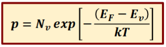
Hole concentration in valence band formula (intrinsic)
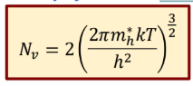
Effective density of states at valence band edge (intrinsic)
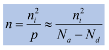
Mass action Law
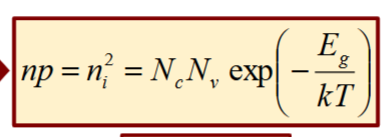
When can we use the mass action law?
At thermal equilibrium
dark (no illumination)
applies to both intrinsic and extrinsic semiconductors
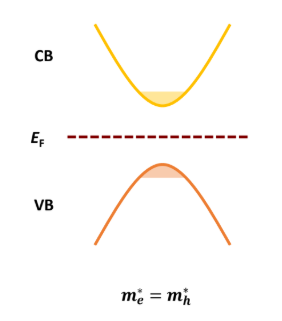
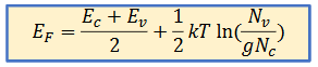
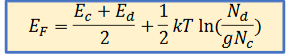
Fermi Energy for intrinsic semiconductors
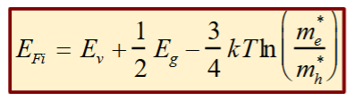
Fermi Energy for intrinsic semiconductors if if Nc = Nv, or me* = mh*
In the middle of the band gap
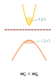
Where is Fermi Energy for intrinsic semiconductors if me* < mh*
Above the middle of the band gap
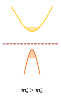
Where is Fermi Energy for intrinsic semiconductors if me* > mh*
Below the middle of the band gap
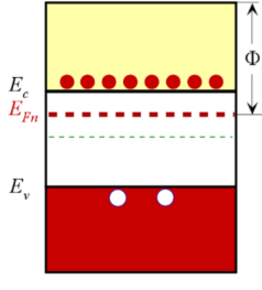
Fermi level for n-type semiconductor
closer to the conduction band
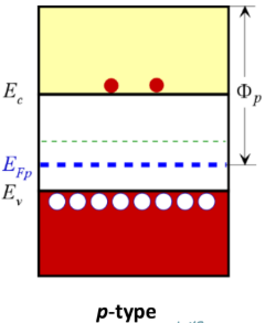
Fermi level for p-type semiconductor
closer to the valence band
Elements that are electron acceptors (p-type dopants)
Group 13 elements (boron, aluminum, gallium, indium…)
Elements that are electron donors (n-type dopants)
Group 15 elements (phosphorous, arsenic, antimony…)
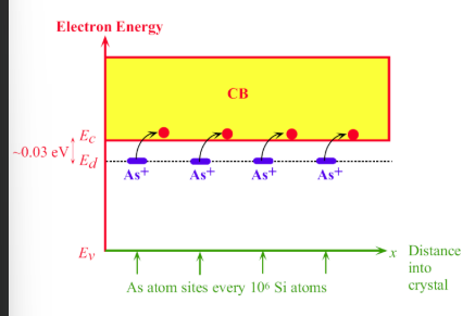
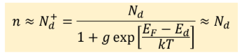
N-type doping
donor energy levels are just below Ec around ionized donor sites
Thermal excitation at room temperature can ionize donors and donates a free electron in conduction band
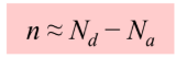
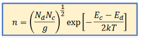
Donor atom concentration is often much higher than ni so thus n ≈
Nd
hole concentration is really small
Assumptions we can make with n-type doping
At RT, donors are fully ionized: Nd ≈ Nd+
Heavy doping: Nd ≫ ni
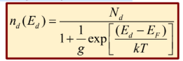
General expression for concentration of Occupied Donors:
g is typically 2 for donors
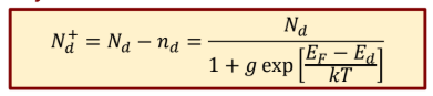
General Expression for Concentration of Ionized Donors at T:
g is typically 2 for donors
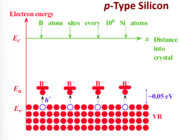
P-type doping
Acceptor energy levels just above Ev around ionized acceptor sites
Thermal excitation at room temp can excite electron into acceptor level, and create a free hole in valence band
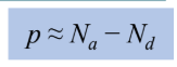
acceptor atom concentration often much higher than pi,so p ≈ Na
electron concentration in CB is small
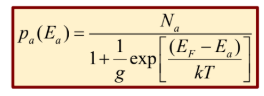
General expression for concentration of Occupied Acceptors:
usually g = 4 for acceptors
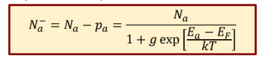
General Expression for Concentration of Ionized Donors at T:
usually g = 4 for acceptors
Compensation doping
doping semiconductor with both donors and acceptors
Majority carrier for n-type compensation doping
minority carrier for n-type compensation doping
Majority carrier for p-type compensation doping
minority carrier for p-type compensation doping
General expressions for compensation doping
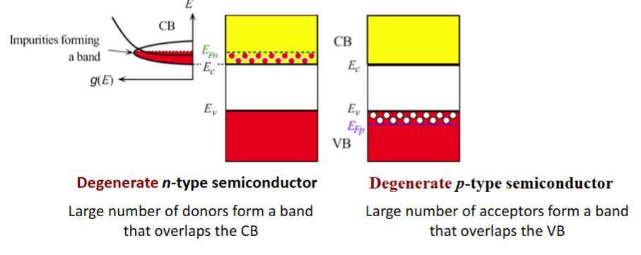
Degenerate semiconductors
semiconductor is excessively doped, where n or p is comparable or greater than Nc or Nv
Becomes more metal-like than semiconductor like
larger number of donors/acceptors form band overlapping with CB/VB
No longer valid: (i) Mass action law; (ii) Boltzmann approximation
Need to use: (i) Fermi-Dirac statistics; (ii) Sommerfeld model.
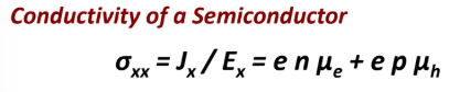
Conductivity of semiconductor
Current density of a semiconductor
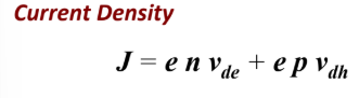
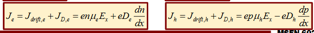
Electron and hole drift velocities
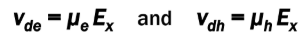
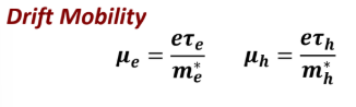
Electron and hole drift mobilities
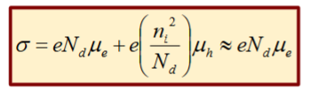
n-type conductivity
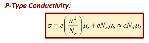
p-type conductivity
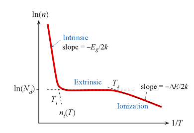
Temperature Dependence of conductivity plot
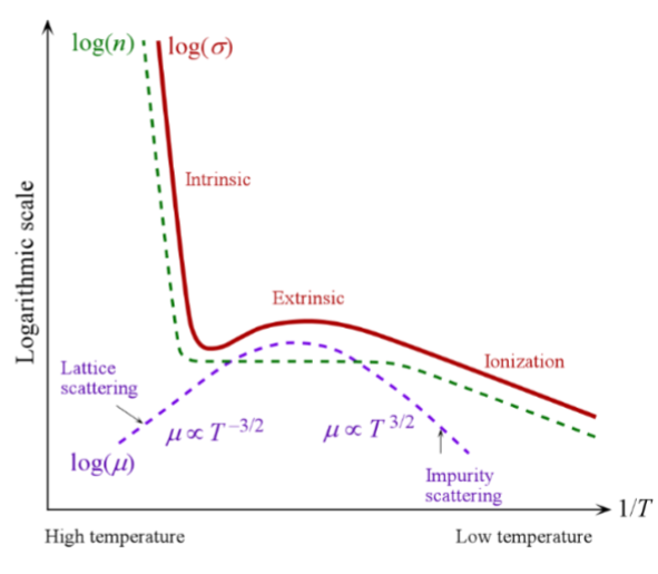
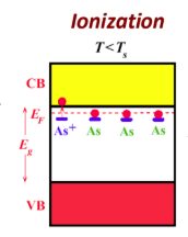
behavior below saturation temperature (n-type)
electron concentration is controlled by the ionization of the donors (via thermal excitation of electron from Ed to Ec).
n ≈ Nd+
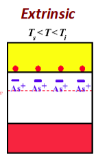
behavior between saturation temperature and intrinsic temperature (n-type)
electron concentration is equal to donor concentration due to full donor ionization
n ≈ Nd+ ≈ Nd
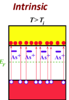
behavior above intrinsic temperature (n-type)
thermally generated electrons from VB to CB exceed the number of electrons from ionized donors, semiconductor behaves as if its intrinsic
ni >>Nd
Temperature dependence of electron concentration (n-tyoe)
electron concentration for high temp n-type semiconductor
The doped semiconductor behave like intrinsic semiconductor.
Fermi level for high temp n-type semiconductor
The carrier concentration is fully controlled by the doping concentration.
electron concentration for room temp n-type semiconductor
The carrier concentration is fully controlled by the doping concentration.
electron concentration for low temp n-type semiconductor
The doped semiconductor behave as if Ed is the “valence band”
Fermi level for high temp n-type semiconductor
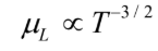
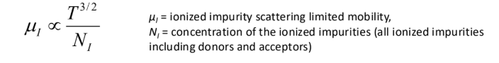
2 sources of temp dependence drift mobility
Scattering of electrons by lattice vibrations at high T
scattering of electrons by ionized impurities at low T (columbic potenital from ion scatters electrons)
Lattice Scattering Limited mobility
Effective at high temps
higher temps increase scattering cross section (S) which reduces drift mobility
Ionized impurity scattering limited mobility
Effective at lower temperature
higher temps reduce scattering cross sections which increases drift mobility
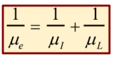
Effective mobility
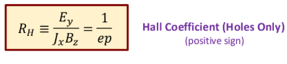
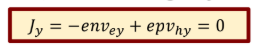
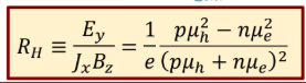
Hall coefficient for holes only
What must the net force applied to each electron or hole must be equal to under steady state in the hall effect
0
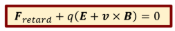
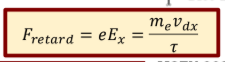
Formula for retarding force in hall effect
what should the current along the y direction be equal to in the hall effect at steady state
0
Ambipolar hall coefficient
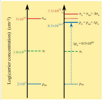
Effect low level photo injection has on charge carriers in n-type
does not significantly affect majority nn
but it drastically affects the minority pn
What determines the recombination time of excess carriers during photo injection
Minority carrier lifetime
Excess Minority Carrier Concentration in n-type semiconductor =
what does a short Minority carrier lifetime mean?
fasts switching pn junction
what does a long Minority carrier lifetime mean?
persistent luminescence
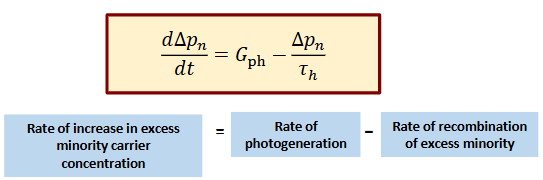
Stages in transient photoconductivity
Thermal Eq: carriers and lattices are interacted with one another ONLY through thermal excitation for long enough time, homogenous fermi level.
Transient: excess carriers are generated (for example, under illumination), and evolve with time.
Steady State: the external excitation is applied for long enough time until the excess carriers no longer change with time. It is still a non-equilibrium state, and the Fermi energy is not constant throughout the system.
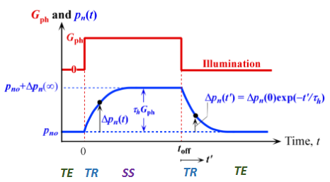
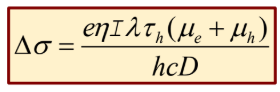
Equation for steady state photoconductivity
η is quantum efficiency (# of electrons generated per incident photon)
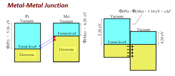
Metal Metal Junctions
electrons from higher lvl tunnel to metal with lower fermi lvl
tunneling occurs until the fermi lvls across both metals are equal
at equilibrium, there is a contact potential across the interface
Band bending under E field for electrons
drift opposite direction of electric field
As V(x) decreases, electron PE increases
Band bending under E field for holes
drift same direction of electric field
As V(x) increases, hole PE decreases
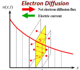
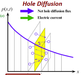
Flux density

Fick’s first law
electrons and holes diffuse from high-concentration regions to low-concentration regions.

Diffusion current density
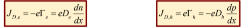
Electron Diffusion and electric current
in opposite directions
Hole Diffusion and electric current
in same direction
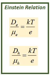
Einstein Relations
Total current density
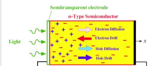
diffusion and drift directions for photo excitation at the left side of semiconductor
Electron diffusion (flux): to the right
Hole diffusion (flux): to the right
Electron diffusion current: to the left
Hole diffusion current: to the left
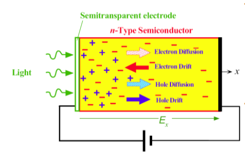
diffusion and drift directions for photo excitation at the left side of semiconductor with E field left to right
Electron drift (flux): to the left
Hole drift (flux): to the right
Electron drift current: to the right
Hole drift current: to the right
Ideal PN Junction
band bends and causes contact potential with e field pointing towards p side
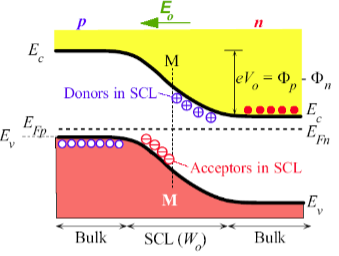
Transport of electrons and holes in p-n junction
Electron Diffusion: to the left
Electron drift: to the right
Hole diffusion: to the right
Hole drift: to the left
No net current
Continuity Eq for holes in n-type
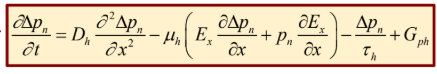
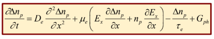
Continuity Eq for electrons in p-type
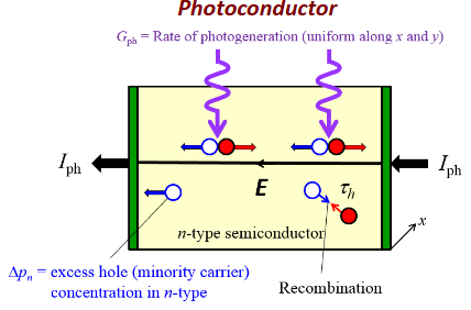
Photoconductor with surface photogeneration
Assumptions:
(1) Infinitely long semiconductor
(2) Steady states: ∂/∂t = 0
(3) Negligible electric field: Ex ~ 0
(4) Surface photogeneration: Gph ≠ 0 only when x = 0
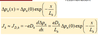
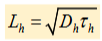
Diffusion length
The mean distance diffused by the excess carriers before recombination.
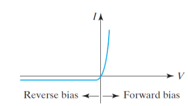
Bias graph for pn diode
Space charge region
region near a p-n junction depleted of mobile carriers, leaving behind fixed charged ions.
contains net charge from immobile ions
creates the electric field
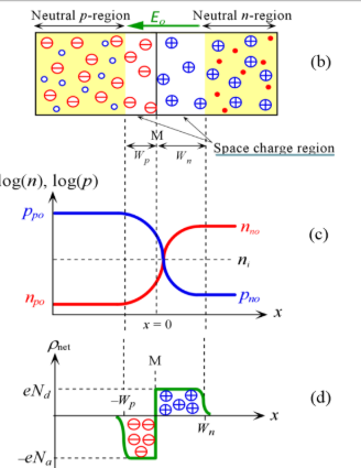
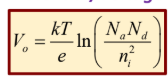
Built in Potential/Voltage from SCR
Forward bias on PN junction
EFp shifts down away from EFn
p and n side bands shift relative (closer) to each other (less bending)
built in potential and depletion width decreases
net current from p to n
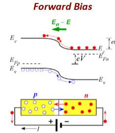
hole and electron drift and diffusion for forward bias of PN diode
Electron Diffusion: Larger and to the left (less of a barrier)
Electron Drift: Smaller and to the right (because potential is smaller)
Hole diffusion: Larger and to the right
Hole Drift: Smaller and to the left
Net current: to the right (n side)
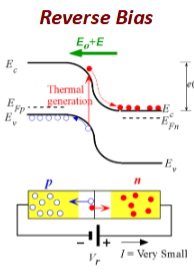
Reverse bias on PN junction
EFp shifts up away from EFn
p and n side bands shift relative (away) to each other (more bending)
built in potential and depletion width increases
net current from n to p