Chapter 5 Thin-Film Transistor Flat-Panel Array Image Acquisition
1/91
There's no tags or description
Looks like no tags are added yet.
Name | Mastery | Learn | Test | Matching | Spaced | Call with Kai |
|---|
No analytics yet
Send a link to your students to track their progress
92 Terms
Indirect Conversion
Introduction
thin-film transistor (TFT)
flat-panel amorphous silicon and amorphous selenium (a-Se)
were the first devices to move beyond the cassette into detectors that would reside in the table and wall stan
Introduction
What are flat-Panel detectors
the materials used for detecting the X-ray signal
Introduction
The sensor of the flat-panel detector are enclosed where
rigid protective housing
Active-Matrix Flat-Panel Imagers
Active-matrix flat-panel imagers (AMFPI) consist of
a flat-panel array with an X-ray absorption material.
Active-Matrix Flat-Panel Imagers
The two main types of x-ray absorption materials
photoconductors and scintillators.
Active-Matrix Flat-Panel Imagers
What is a photoconductor
are materials that absorb X-rays, resulting in an electrical charge
Active-Matrix Flat-Panel Imagers
What is a scntillator
phosphors that produce light when absorbing x-ray
Active-Matrix Flat-Panel Imagers
What is the function of AMFPI
measures the response of these materials to X-ray absorption and is a large area two-dimensional (2-D) array of pixels
-fastened to glass
What is the function of ( 2-D) array of pixels
device that measures X-ray absorption rather than counting or measuring the actual X-rays.
The choice of x-ray absorption material determines
whether the detector uses direct or indirect signal conversion
Active-Matrix Flat-Panel Imagers
What is the absorption material that is attached to the surface of the array of pixels
electrically(photoconductor) or
physically (phosphor material)
Direct Conversion
What happens in direct conversion
X-ray photons are absorbed by the coating material and immediately converted into an electrical signal
direct conversion
The flat-panel detector has a radiation-conversion material or ________________
photoconductor
direct conversion
The flat-panel detector has a radiation-conversion material or ________________ , is typically made of what material
(a-Se)
Amorphus selenium
direct conversion
Function of (a-Se)
material absorbs X-rays and converts them to electrons, which are stored in the TFT detectors
direct conversion
During conversion process of
(a-se) x-rays are converted to electrons... where are the electrons stored
In TFT detectors
direct conversion
What is TFT?
a photosensitive array made up of small pixels, also called a detector element (del) in these TFT arrays
direct conversion
TFT is a photosensitive array made up of small pixels called DEL's, Each of the pixels contains ____________
a photodiode
direct conversion
What is the function of the photodiode
that absorbs the electrons and generates electrical charge
direct conversion
Wht is the function of field effect transistor (FET) or silicon TFT
isolates each pixel element and reacts like a switch to send the electrical charges to the image processor
1 million pixels can be read and converted to a composite digital image in less than 1 second
direct conversion
What are TFT switches
line of TFT switches each associated with a storage capacitor, allows the electrical charge information to discharge when the switches are closed
direct conversion
TFT switches allow electrical charge information to discharge when swicthes are closed... where is the information discharged to/onto
data columns and read out with dedicated electronics.
direct conversion
Specialized silicon integrated circuits are connected where
connected along the edges of the detector matrix
Direct conversion
Specialized silicon integrated circuits...... On one side, integrated circuits control the ____________
On the other side, low-noise, highsensitivity amplifiers perform___________(3 things)
line scanning sequence
the readout, amplification, and analog-to-digital conversion
Direct conversion
After the Specialized silicon integrated circuits finish its processes what happens next
High-speed digital electronics are then used to achieve fast image acquisition and processing
Indirect Conversion
Indirect conversion is similar to direct conversion how
In the use of TFT array
Indirect Conversion
Indirect Conversion is different from direct conversion how
Indirect is a 2 step process
Indirect Conversion
What is the 2 step process?
1. X-ray photons are converted to light
2. Light photons are converted to electrical signal
Jargon....
Step 1:X-ray photons striking the dielectric receptor are absorbed by a scintillation or phosphor material in the imaging plate that converts the incident X-ray photon energy to light
Step 2: A photosensitive array, made up of small (about 100 to 200 µm) pixels, converts the light into electrical charges. Each pixel contains a photodiode that absorbs the light from the scintillator and generates electrical charges. A FET or silicon TFT isolates each pixel element and reacts like a switch to send the electrical charges to the image processor. As with direct conversion, more than 1 million pixels can be read and converted to a composite digital image in less than 1 second
Indirect Conversion
Phosphor Based Scintillatiors- also known as
The scintillation Layer
Indirect Conversion
What are the two types of phosphor based scintillation materials
phosphor such as gadolinium oxysulfide (Gd2O2S), or thallium-doped cesium iodide (CsI[TI])
Indirect Conversion
What is the function of the gadolinium oxysulfide (Gd2O2S), or thallium-doped cesium iodide (CsI[TI]) scintillation layer
absorbs xrays and produces light.
Indirect Conversion
In what two ways can the two can the scintillation layer be composed
structured or unstructured
Indirect Conversion
Characteristics of a unstructured scintillation layer
produce more scattered light than structured layers, thereby decreasing the efficiency of the detector.
Indirect Conversion
Process of Conversion
1. Phosphor Based Scintilator (x-rays & produce light)
Next
2. Photodetector ( detects light then converts to electrical charge )
Indirect Conversion
What material is the photodetector made of
hydrogenated amorphous silicon (a-Si:H) photodiode array
Indirect Conversion
phosphor based scintillation material= gadolinium oxysulfide has a scintllation layer of small crystals bound together how
unstructured or turbid (powdered granules)
Indirect Conversion
phosphor based scintillation material(gadolinium oxysulfide)
has a crystalline layer filled with air pockets that allow light generated in the phosphor to escape laterally before it reaches the surface
What is the downside of this?
reduces the efficiency of the phosphor and lowering spatial resolution
Indirect Conversion
phosphor based scintillation material cesium iodide (CsI) scintillator.
The most common type of phosphor based scin material is
cesium iodide (CsI) scintillator.
Indirect Conversion
phosphor based scintillation material cesium iodide (CsI) scintillator.
The Scintillation Layer of Cesium Iodide is composed how
Because of how the CsI crystals are grown ( perpendicular to the detector surface; crystalline needles work as light-directing tubes) they are considered a structured scintillator
Indirect Conversion
phosphor based scintillation material cesium iodide (CsI) scintillator.
Is cesium iodide better than gado oxy and why
Greater DQE and there there is no light spread
Indirect Conversion
phosphor based scintillation material cesium iodide (CsI) scintillator.
No light spread=
higher spread resolution
Indirect Conversion
phosphor based scintillation material cesium iodide (CsI) scintillator.
Perpendicular crystaline needles absorb (x-rays & convert energy into light) the light is channeled to the
amorphous silicon photodiode array
Indirect Conversion
phosphor based scintillation material cesium iodide (CsI) scintillator.
Today because of the advances in materials and crystalline formation on the array, both CsI and Gd2O2S are being used in portable detectors.
In the past the crystaline structure was too delicate to be used outside of the protected enviornment of a fixed detector array
Flat-Panel Array Design and Performance
Design
The way an a-Si:H array functions is very complex; however, the design is fairly simple. Each pixel contains a
sensing component and a switching component
Flat-Panel Array Design and Performance
Design
What are the two types of switching components
1. 2 contact switching diode
2. 3 contact TFT
Flat-Panel Array Design and Performance
Design
The choice of switching components depends on
depends on the type of absorbing material and the vendor's choice of construction.
Flat-Panel Array Design and Performance
Design
A phosphor/scintillator requires a ______________ to detect light
photodiode or phototransistor
Flat-Panel Array Design and Performance
Design
If a photoconductor (a-Se) is selected, the sensing element is a __________
capacitor
Flat-Panel Array Design and Performance
Design
If a photoconductor (a-Se) is selected, the sensing element is capacitor that measure _________
charge
Flat-Panel Array Design and Performance
Design
To operate, the flat-panel detectors use about 2.5 km or 1.6 miles of electrical bias (a predetermined amount of voltage or current in an electrical circuit), control, and signal output lines laid out on the array surfaces so that each pixel is monitored and refreshed during the control and reading process. Each row of pixels is connected to the same horizontal control line, and each column is connected to the same vertical data line. The readout electronics are attached to the edges of the array, and the entire array and its components are enclosed in a protective housing.
Flat-Panel Array Design and Performance
Design
When the exposure is made, the sensing/storage component within the pixel contains the image information. The information is then read out line by line via the changing of the control line voltage so each pixel is connected to its corresponding data line at the bottom of the column
Flat-Panel Array Design and Performance
Design
Once the exposure is made
Sensing component within the pixel contain image info
Fig. 5.7A illustrates the detector in its initialized state, prepared and waiting for exposure. In Fig. 5.7B, the detector has been exposed and is awaiting reading of the array. Fig. 5.7C demonstrates the readout or release of signal of row 1. Notice that a voltage is applied across the control or switch line corresponding to row 1. In the final image of Fig. 5.7, row 1 has returned to an initialized state (the process of returning to this state varies per vendor and is beyond the scope of this textbook) after release of its signal and the readout process continues to row 2. Once the signal has been released, the energy is then transferred to the electronics that are attached to the edges of the array.
Detector Performance
How is detector performance measured
1. Numerical measurement of spatial resolution & DQE
2. Observation of low contrast objects in a contrast detail phantom
Detector Performance
current performance measurement of signal to-noise ratio and DQE indicate that ____________________ perform better than other digital imaging systems. Remember, this is really about efficiency and not resolution
a-Si:H
What is detective quantum efficiency
is a measurement of the efficiency of an image receptor in the converting the x-ray exposure received to a quality radiographic image
What is the relationship between DQE and exposure
The higher the DQE, the lower the radiation exposure to produce a quality image, therby decreasing patient exposure
What is signal to noise ration (SNR)
A method of describing the strength of the radiation exposure
(signal) in the comparison to the amount of noise apparent in the digital image.
What is the relationship of SNR & the amount of noise
(Increasing the SNR means that the strength of the signal is high compared to the amount of noise)
Relationship between SNR & the amount of image quality
Increased SNR= improved quality of the digital image
Relationship between Increased Noise and visibility of anatomic detail
Increased Noise- Decreased visibility of anatomic details
What is contrast to noise ratio
A method of describing the contrast resolution compared with the amount of noise apparent in digital imaging
What is the relationship between CNR and the visibilty of anatomic details
Increasing CNR increases the visibility of anatomic details
The Digital Image
Regardless of the type of digital image receptor, the varying electrical signals are sent to the ADC for conversion of digital data
The digitized pixel intensifies are patterened in the computer form the image matrix
The image matrix is a digital composite of the varying x-ray intensities exiting the patient
Each pixel has a brightness level representing the attenuation of chracteristics of the volume if tissue images
Flat-Panel Artifacts
What are the 3 types of flat-panel artifacts
1.Dead Pixels
2.Incorrect Gain Cali
3.Image Lag & Incorrect Offset Orientation
Flat-Panel Artifacts
Dead Pixels
There is a possibility in imaging systems ______________ image information due to defects
misrepresenting/ losing
Flat-Panel Artifacts
Dead Pixels
Artifacts can be cause how?
by malfunctions
Flat-Panel Artifacts
Dead Pixels
As detector ages more dead pixels are located where
located on the edge
Flat-Panel Artifacts
Dead Pixels
What are some reasons or malfunctions that will result in defective pixels
Dust, scratches, static discharge, chemical corrosion, or interactions between materials can occur
Flat-Panel Artifacts
Dead Pixels
As the detector ages, the number of dead pixels increases but may not be detected if they are located
on the edges of the panel.
Flat-Panel Artifacts
Dead Pixels
Manufacturers make efforts to maintain a standard of less than approximately _______________
0.1% to 0.2% defective pixels
Flat-Panel Artifacts
Dead Pixels
What software is used to fill in dead pixels called
Interpolation method
Flat-Panel Artifacts
Incorrect Gain Calibration
Gain Calibration is used for what reason
used to correct flaws in the detector.
Flat-Panel Artifacts
Incorrect Gain Calibration
What are the two ways a noticeable artifacts can be seen
If an area of the detector has a large number of dead pixels or if there is an area of the detector that has poor connections between the conversion layer and the a-Si/TFT array
Flat-Panel Artifacts
Incorrect Gain Calibration
To remove the potential of having that artifact interfere with diagnosis, a process known as ____________ or ____________
gain calibration or flat fielding is used
This process will remove these densities on the image by creating a mask of those defects
Flat-Panel Artifacts
Incorrect Gain Calibration
When a subsequent image is taken, the software will use the 1._____________ to remove the unwanted densities and leave only the 2._______________.
mask
diagnostic information
Flat-Panel Artifacts
Incorrect Gain Calibration
Gain calibration should be performed under the same or similar circumstances in which clinical images will be taken. The calibration should be done according to the equipment manufacturer's guidelines.
Flat-Panel Artifacts
Incorrect Gain Calibration
In the automatic exposure control (AEC) cells appear as slightly positive squares in the image. The gain calibration was performed with the detector outside of the Bucky and then a subsequent image was taken with the detector in the Bucky. This could happen if anything is left on the detector during a gain calibration. These faint marks could lead to a misdiagnosis.

Flat-Panel Artifacts
Image Lag and Incorrect Offset Correction
What is Image Lag
flat-panel systems can take images faster than the detector can accommodate. If an image is taken prior to the detector releasing all of the signal from the previous image, a faint image of the previous exposure may be visible
Flat-Panel Artifacts
Image Lag and Incorrect Offset Correction
How does image lag occur
Almost a double exposure of sorts.. when the detector is unable to get rid of all signal from previous image
Flat-Panel Artifacts
Image Lag and Incorrect Offset Correction
Reason Lag may occur? (2)
-Read succession of image is only one reason
-Lag might occur if overexposure or an area with little beam attenuation such as a techs lead marker
Flat-Panel Artifacts
Image Lag and Incorrect Offset Correction
Techniques to reduce Lag(3)
-Increase the amount of time between exposures giving the detector sufficient time to release all of the residual image
-Reduce the amount of attenuated beam by collimating as clearly as allowable
-Set appropriate technical factors for each body part being examined. If multiple examinations are being done, acquire the image requiring the highest technical factors last.
Flat-Panel Artifacts
Image Lag and Incorrect Offset Correction
Image Lag can also be corrected
How?
can be corrected with the detector's software using the dark noise or offset correction.
Flat-Panel Artifacts
Image Lag and Incorrect Offset Correction
Offset correction
If an offset correction is performed prior to residual signal leaving the pixels, that information will be stored as inherent and could cause a negative image of the residual signal.
Flat-Panel Artifacts
Image Lag and Incorrect Offset Correction
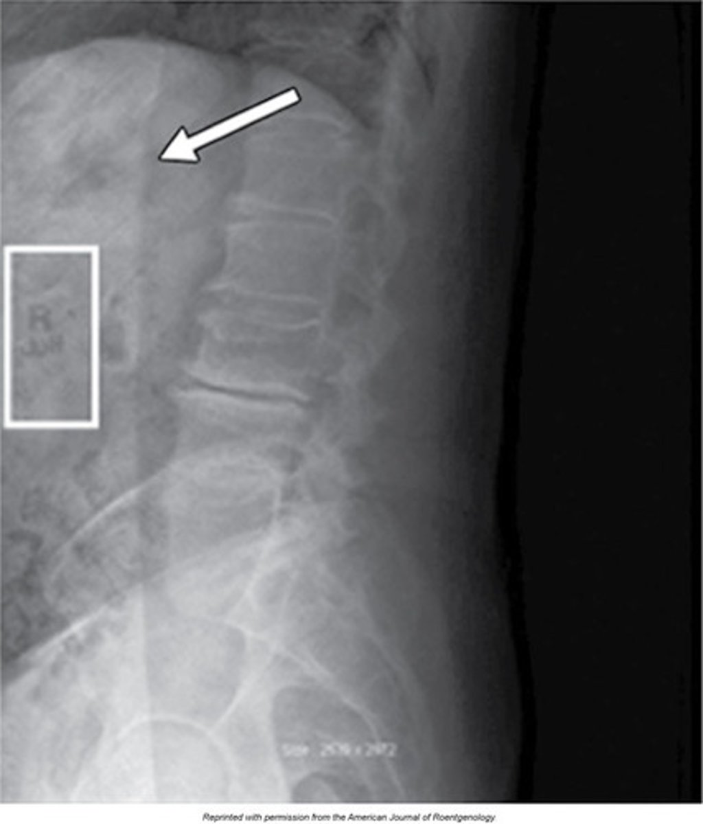
For example, in an offset correction was performed after an examination was done with a right-side marker in an area of unattenuated radiation. Residual signal remained in that area and a subsequent offset correction was performed. The R is now viewed inversely because that signal created a mask during the offset correction. In Fig. 5.10 it is clear that the signal is still very strong and this image was taken 10 minutes after the initial exposure.
For example, in an offset correction was performed after an examination was done with a right-side marker in an area of unattenuated radiation. Residual signal remained in that area and a subsequent offset correction was performed. The R is now viewed inversely because that signal created a mask during the offset correction. In Fig. 5.10 it is clear that the signal is still very strong and this image was taken 10 minutes after the initial exposure.
Emerging Technology
Back in the days tomo was used
Emerging Technology
Describe how tomo machines are constructed.
Tomograms were acquired by attaching a fulcrum to the Bucky and tubehead. The Bucky and tubehead would move in concert with one another and the tube would arc across the patient
Emerging Technology
fulcrum point determines what
determine the area in the body imaged.
This same concept is now being used in digital imaging and it is called tomosynthesis
Emerging Technology
Tomosynthesis is possible with what type of advances
advances in the selenium detector and amorphous silicon TFT arrays,
Emerging technology
During tomosynthesis how fast can images be acquired
rate of 30 frames per second.
Emerging Technology
After the acquisition of entire set of frames required for the part
the frames are sent to a postprocessing workstation for reconstruction
The images are then sent to a viewing station as a stack of images similar to a stack of computed tomography (CT) images
Emerging Technology
When is tomosyn used
in breast imaging for patients with dense breast & has been used on musculoskeletal imaging, with limited use