Electricity-4
1/17
Earn XP
Description and Tags
Semiconductors
Name | Mastery | Learn | Test | Matching | Spaced | Call with Kai |
|---|
No analytics yet
Send a link to your students to track their progress
18 Terms
distinguish between intrinsic and extrinsic conduction in a semiconductor
intrinsic is through a pure semiconductor, while extrinsic is through a doped one
intrinsic has an equal number of holes and electrons but extrinsic has an excess of electrons or holes
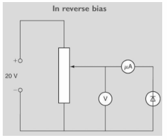
how would you arrange a circuit diagran to show how voltage and current are measured for a diode in reverse bias
what is a semiconductor
a substance whose resistivity is between that of a good conductor and a good insulator
how can a pure semiconductor be converted into a p-type semiconductor. Give an example
an impurity that produces extra positive hole which are available for conduction is added ( a group 3 element is added). Boron added to silicon
how can a pure semiconductor be converted into an n-type semiconductor. GIve an example.
an impurity that produces more free electrons which are available for conduction are added ( a group % element is added). Phosphorous added to silicon
what is the function of a rectifier
a rectifier converts a.c. to d.c
what propertry of a diode makes it useful in a rectifier circuit
diodes allow current to flow in one direction only
explain how a diode might be protected from having too large a current flowing thorugh it when it is connected across a battery
a large resistor should be placed in series with the diode
distinguish between conductors insulators and semiconductors
conductors are good at allowing current to flwo. insulators are poor at allowing current to flow. semiconductors are in-between the two.
what is meant by doping
the addition of a small amount of another element to pure semiconductor to increase its conductivity
describe a depletion layer and explain how it forms
at the junction of the p-type and n-type material, electrons diffuse across from the n-type region to the p-type region. positive holes diffuse from the p-type to the n-type region. the migrating electrons combine with holes and effectively cancel out. due to the loss of mobile charge carriers on either side of the junction, the region is referred to as the depletion layer.
why might it be necessary to place a resistor in series with a diode
to protect the diode by reducing current.
why does the p-n junction in silicon become a good conducot as the potential difference exceeds 0.6V.
The diode becomes a good conductor when the width of depletion layer is reduced to nothing, which happens when voltage exceeds .6V
Explain why the presence of phosphorus and boron makes silicon a better conductor.
phosporus is a group 5 element which makes more free electrons available for conuction,
boron is a group 3 element which means that when added to silicon more positive holes are available for conuction.
describe what happens at the boundary when the semiconductor diode is forward biased
the width of depletion is reduced, making it a conuductor
describe what happens at the boundary when to semiconductor diode is reverse bias
the width of depletion layer increased, so that no conduction can take place.
Give a use of a semiconductor diode
rectifiers
LED
what is a p-n junction
where a p- type semiconductor and an n-type semiconductor meet