Defects
 Call Kai
 Learn
 Practice Test
 Spaced Repetition
 Match
 Flashcards
 Knowt Play
1/16

There's no tags or description
Looks like no tags are added yet.
17 Terms
Point Defect
0-D
Vacancies, interstitials, substitutional impurities, Schottky defects, Frenkel defects
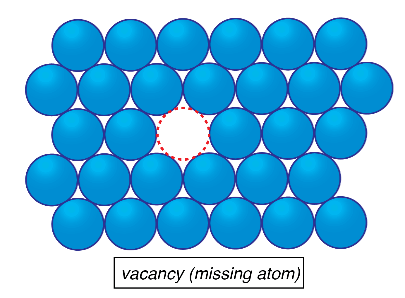
Vacancies
Type of point defect
Empty spaces in lattice
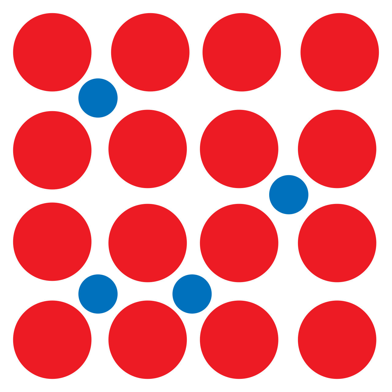
interstitials
Type of point defect
Atoms that fit between the spaces in the lattice
Substitutional Impurities
Type of point defect
Atoms that replace others in the lattice
The defect atoms usually not the same size which generates internal lattice strain
Non-equilibrium bond lengths


Line Defect
1-D
Edge dislocations, screw dislocations
A ‘line’ of atoms that is misplaced
Planar defect
2-D
Grain boundaries, stacking faults, interphase boundaries, surfaces

Grain boundaries
2-D
marks the interface where two differently oriented crystals (called grains) meet in a polycrystalline material
Why is defect formation is a thermally unfavorable process?
It raises the free energy of a system by adding enthalpy
Takes energy to break chemical bonds
Why do defects form?
Entropy
The random location of point defects in a material increases the randomness (entropy) in a system, thereby lowering free energy and making them thermodynamically favorable to form
Gibbs free energy equation and how each element affects G
ΔG = ΔH - TΔS
ΔG → tells us whether the reaction will be spontaneous or not
Spontaneous when ΔG is negative
ΔH → enthalpy; increasing H makes G less negative
barrier to the process
ΔS → entropy; the amount of randomness
increasing S makes G more negative
How does Electronic Doping work?
the intentional addition of trace impurity atoms into a pure semiconductor crystal (like silicon) to drastically increase its electrical conductivity and control how it carries current
N-type electronic doping
Group V elements with 5 valence electrons—such as phosphorus or arsenic—are added to silicon (which has 4 valence electrons). Four electrons bond normally with the neighboring silicon atoms, leaving an extra free electron behind. These extra electrons move freely and serve as negative charge carriers (majority carriers)
P-type electronic doping
Group III elements with 3 valence electrons—such as boron or gallium—are added to silicon. Because the dopant has one fewer electron than needed, it creates a vacant spot or "hole" where an electron is missing. Electrons from neighboring atoms jump to fill these holes, making the holes move through the material as positive charge carriers (majority carriers).
Solid Solution
If 2 or more elements are of similar size, it is possible to continually add the “impurity” species
Rules for solid solutions (4)
Have atomic radii that are < 15% different from one another in size
Have electronegativity that are compatible to one another
Have the same valence (or similar)
have the same crystal structure
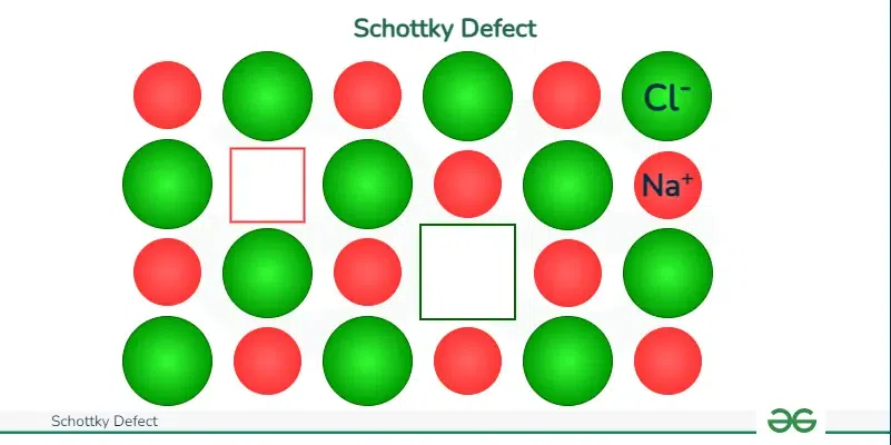
Schottky Defect
Clusters of vacancies
Ratio of anion to cation vacancies will math stoichiometry so that effective charge is zero
Frenkel Defect
Occurs when an atom (ion) is displaces
Creates both vacancy and interstitial
Effective charge is zero
Usually the smaller ion is the one that moves
