IXD 153 LP 05 Terms - second half of semester
 Call Kai
 Learn
 Practice Test
 Spaced Repetition
 Match
 Flashcards
 Knowt Play
1/25

Earn XP
Description and Tags
STUDY OBJECTIVES Introduce the use of diodes and rectifiers as voltage dropper, voltage regulation, reverse polarity protection, adjustable attenuator, audio limiter, AC-DC rectification, voltage doubler and voltage quadrupler.
26 Terms
Diodes and rectifiers
electronic components that conduct electricity in one direction only
Forward Bias
The orientation of the diode in a circuit to conduct voltage and current.
Biasing of a diode in a schematic circuit can be determined by the position of the ‘banded collar’ that determines the direction of voltage and current either passing through, or blocked, by the diode.
Reverse Bias
The orientation of the diode in a circuit to block voltage and current.
Biasing of a diode in a schematic circuit can be determined by the position of the ‘banded collar’ that determines the direction of voltage and current either passing through, or blocked, by the diode.
Anode
The through hole conducting lead (TH configuration) or surface mount connector (SMT) of a forward biased diode that receives the voltage to pass through the diode. In a schematic circuit, the diode’s anode conductor is typically identified as pin number 1.
Cathode
The conducting lead or surface connector of a forward biased diode that 'blocks' voltage from passing through the diode. In a schematic circuit, the cathode conductor is typically identified as pin number 2.
Forward Voltage
Vf
The forward voltage is the threshold voltage value that must occur before the diode will begin to conduct electricity. This value is typically between 0.6 - 1.1 volts. Note that this forward voltage drop value must be subtracted from the amplitude of the input voltage rectified by the diode or rectifier.
Reverse Voltage
Vr
In a forward biased diode, the reverse voltage is effectively blocked until a threshold value is exceeded beyond which Ir increases rapidly. The threshold value of Vr is typically several times greater than the Vf value. Therefore, the diode acts as a ‘flow’ valve for voltage and current in the forward direction.
Forward Current
If
When a diode is forward biased it conducts current (IF) in the forward direction. The value of IF is directly dependent on the amount of forward voltage Vf. The relationship of forward voltage and forward current is called the ampere-volt, or IV characteristic of a diode. Forward Voltage is measured across the diode and Forward Current is a measure of current through the diode.
Forward Current
When the forward voltage across the diode equals 0V, forward current (IF) equals 0 mA.
Starting from 0 volts, if VF is progressively increased in 0.1-V steps, IF begins to rise
When the value of VF is large enough a considerable increase in IF occurs. The point at which this occurs is often called the knee voltage VK.
For germanium diodes, VK is approximately 0.3 V, and 0.7 V for silicon.
If the value of IF increases much beyond VK, the forward current becomes quite large.
Forward Current
This operation causes excessive heat to develop across the junction and can destroy a diode. To avoid this situation, a protective resistor is connected in series with the diode. This resistor limits the forward current to its maximum rated value (See manufacturer’s Data Sheet).
A current limiting resistor is normally used when diodes are operated in the forward direction.
Reverse Current
Ir
In a forward biased diode, the reverse current is typically found to be microamperes in magnitude. In general, this means that reverse current remains constant over a large part of reverse voltage.
As the reverse voltage of a diode is increased, there is a very slight change in the reverse current. At the breakdown voltage (VBR) point, current increases very rapidly.
The voltage across the diode remains reasonably constant at this time.
Reverse Current
The constant-voltage characteristic leads to a number of applications for diodes in the reverse bias condition.
The processes responsible for current conduction in a reverse-biased diode are known as Avalanche breakdown and Zener breakdown.
We will study Zener diodes and Light Emitting Diodes (LEDs) more closely in future lesson plans.
Ground is ground
This is always true in analog circuits, however, in the digital domain, both analog and digital grounds may exist in a circuit.
Half-Wave Rectifier
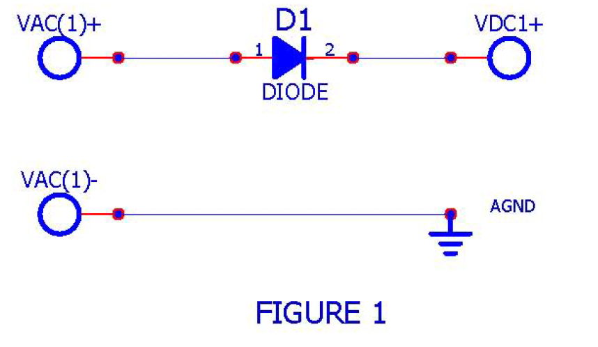
(See FIGURE 1) This circuit accepts an AC input signal and transforms the incoming AC to a half-wave, positive, pulsating DC output signal. Diode must be properly rated for the AC input voltage.
Dual Half-Wave Rectifier
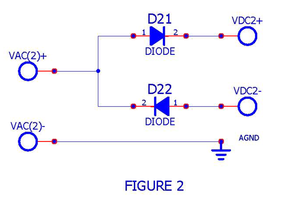
(See FIGURE 2) This circuit accepts an AC input signal and transforms both positive and negative components of the incoming AC to individual half-wave, positive and negative, pulsating DC output signals.
This circuit configuration results in a dual polarity output (pos and neg) that can be used to power dual polarity power components such as op amps.
Full-Wave Bridge Rectifier
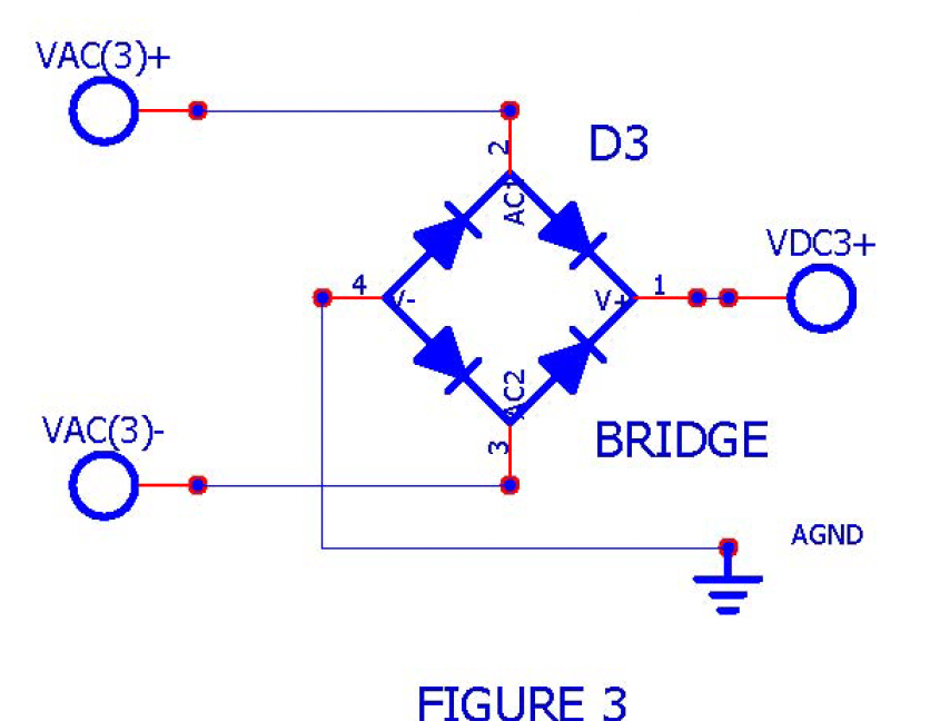
(See FIGURE 3) The bridge rectifier accepts an AC input signal and transforms both positive and negative components of the incoming AC to a full-wave, positive, pulsating DC output signal.
The Bridge Diode can consist of four (4) individual rectifier diodes or an integrated module.
As with the single diode application, the bridge diode must be properly rated for the AC input voltage.
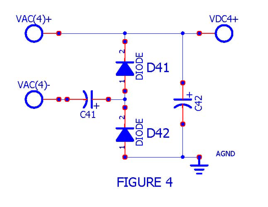
Voltage Doubler
(See FIGURE 4) Similar to Figure 1, however, this configuration will result in a half-wave pulsating DC output that is twice the amplitude of the incoming AC signal.
Note use of a polarized capacitor introduced into the block diagram to reduce ripple current.
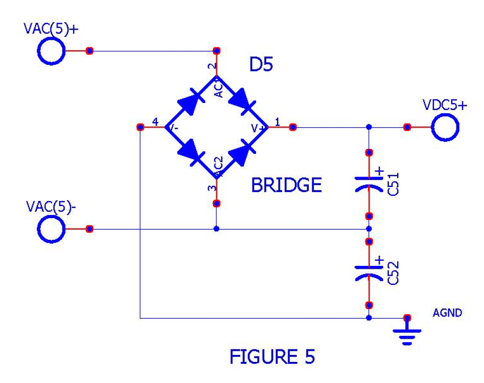
Bridge Rectifier Voltage Doubler
(See FIGURE 5) Similar to Figure 3, however, this configuration will result in a full-wave pulsating DC output that is twice the amplitude of the incoming AC signal.
Note use of multiple polarized capacitors introduced into the block diagram to reduce ripple current.
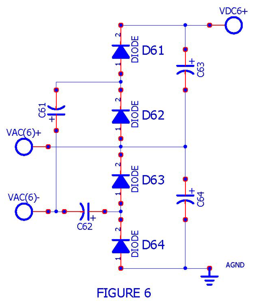
Voltage Quadupler
(See FIGURE 6) Similar to Figure 4 except this configuration will result in a half-wave pulsating DC output that is four times (4x) the amplitude of the incoming AC signal.
Note use of multiple polarized capacitors. Caution, this configuration may result in dangerously high voltages!
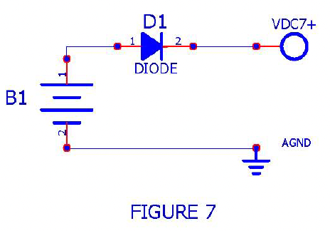
Reverse Polarity Protection
(See FIGURE 7) The diode in this basic circuit protects against the battery bring installed in the reverse direction.
Output from the battery voltage will be reduced by Vf. of the diode.
Transient Protection
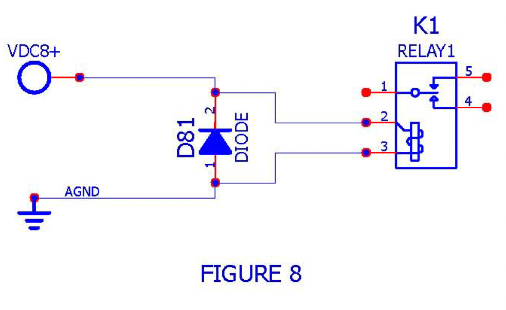
(See FIGURE 8) When the current (I) flowing through an inductor, such as the coil of a relay (see component K1, pins 2,3), is switched off, the magnetic field dissipating in the coil generates a temporary high voltage spike.
A diode installed across the coil in the ‘reverse bias’ direction provides a ‘short circuit’ to protect the rest of the circuit from the high voltage spike.
Adjustable Waveform Attenuator
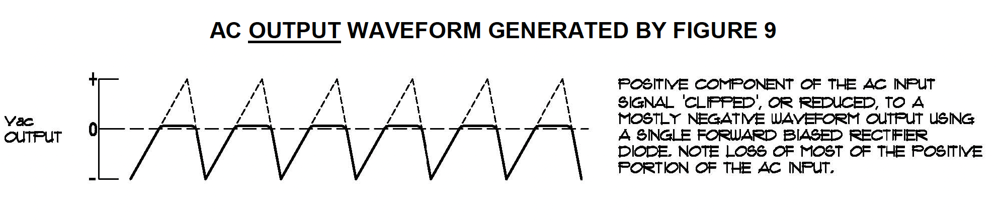
(See FIGURE 9) Adjust the value of resistor ‘R2’ to vary the amount of ‘clipping’ of the AC [triangle] input signal.
The ‘clipped’ output of this circuit is a modification of the [triangle] waveform that removes the positive portion of the triangle waveform that removes the positive portion of the triangle wave form while leaving the negative portion unaffected (for the most part).
The value of +VDC(9) should be a minimum of 1V greater than the P-P input voltage of the AC triangle wave signal.
Dual Polarity Adjustable Waveform Attenuator
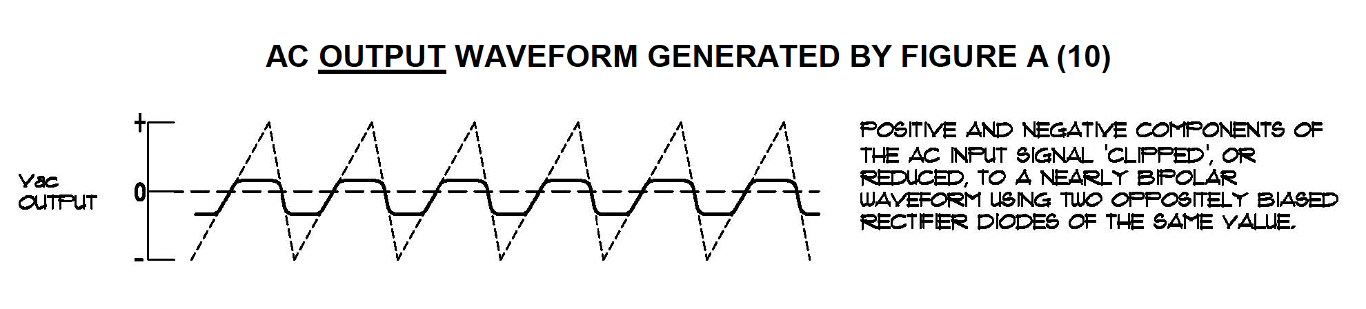
[See FIGURE A (10)] Similar to circuit FIGURE 9 above except this circuit ‘clips’ both the positive and negative portions of the AC triangle input signal.
Adjust the value of resistor ‘VR1A’ to vary the amount of ‘clipping’ of the AC triangle input signal.
The value of +VDC(A) should be a minimum of 1V greater than the P-P input voltage of the AC triangle wave signal.
Audio Limiter
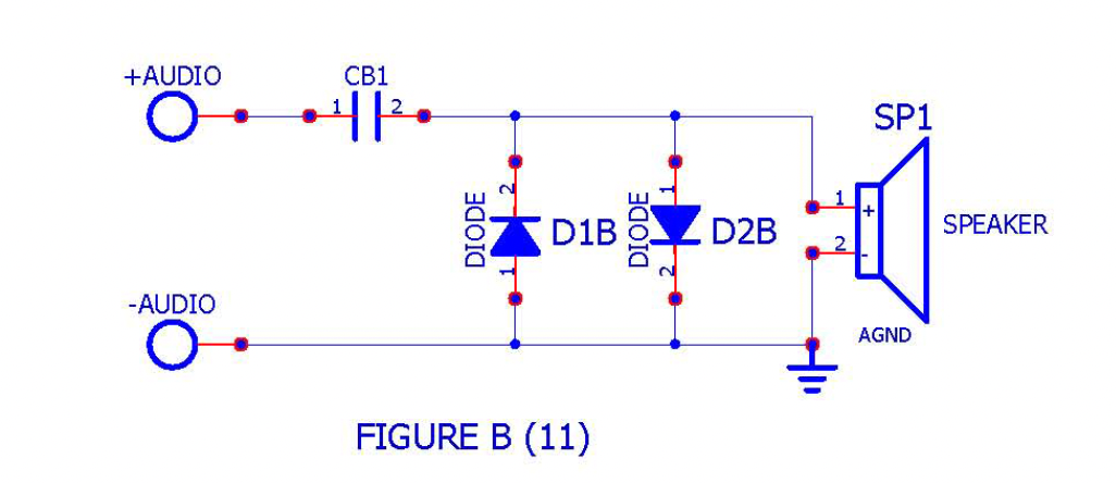
[See FIGURE B (11)] This basic circuit can be used to limit noise, pops, and static.
Can often be found in the circuitry of power amplifiers.
Voltage Reducer
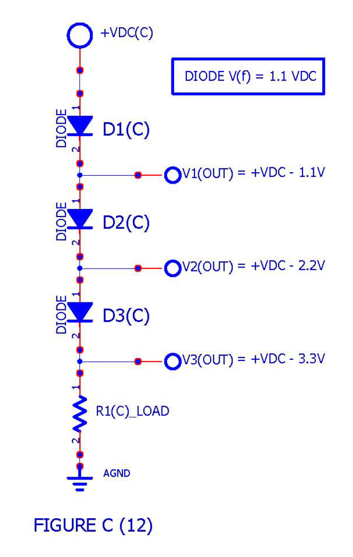
(See FIGURE C (12)
Vdn = Vin – (n * Vf) volts (1)
where:
Vdn = Voltage reduced by EACH diode in the ‘ladder’
Vin = Supply Voltage to the diode ‘ladder’
n = Integer from 0 – n representing the number of diodes in the ‘ladder’
Vf = Reduction due to the forward voltage of each component diode (typically 0.6 -1.1 V)
This circuit can be used to reduce the voltage entering a circuit to a series of smaller output voltages.
Output voltages are limited to increments of the diode’s forward voltage (the amount of voltage needed to get current to flow across a diode).
Voltage Regulator
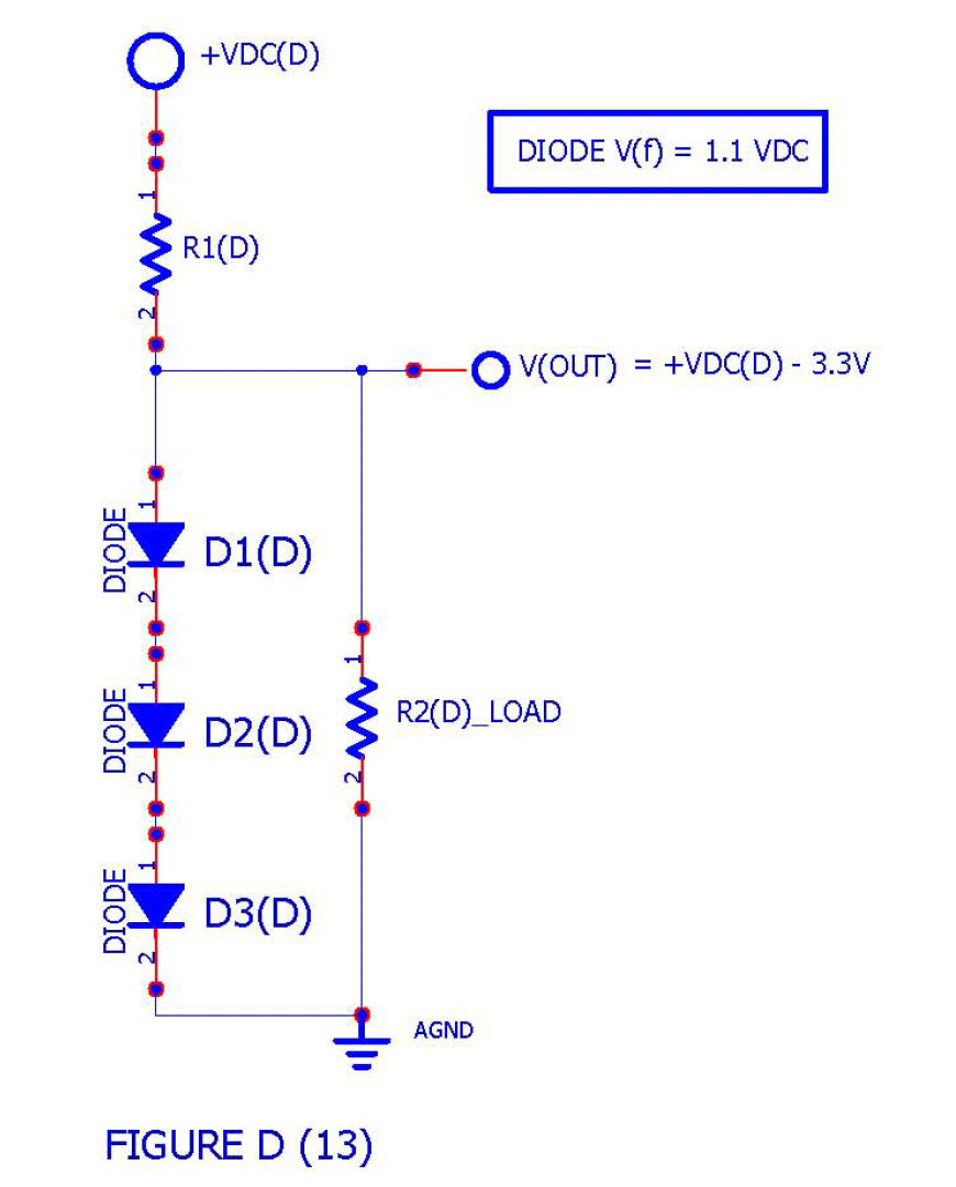
(See FIGURE D (13)
VOUT = Vin – (n * Vf) volts (2)
where:
VOUT = Voltage reduced by the total number of diodes ‘n’ in the ‘ladder’
Vin = Supply Voltage to diode ‘ladder’
n = Total number of diodes in the ‘ladder’
Vf = Reduction due to the forward voltage of the diode component (typically 0.6 -1.1 V)
R1 = (Vin – VOUT) / I Note: determine proper power rating of diodes and resistors using Ohm’s Law
This circuit is a modification of the Voltage Reducer used to supply a single, steady, smaller output voltage from a larger input voltage entering a circuit.
Output voltage is limited to a multiple of the diode’s forward voltage (the amount of voltage needed to get current to flow across a diode).