Processing and Device Technology
 Call Kai
 Learn
 Practice Test
 Spaced Repetition
 Match
 Flashcards
 Knowt Play
1/153

There's no tags or description
Looks like no tags are added yet.
154 Terms
Bipolar Junction Transistor

Timeline of Semiconductor Processing

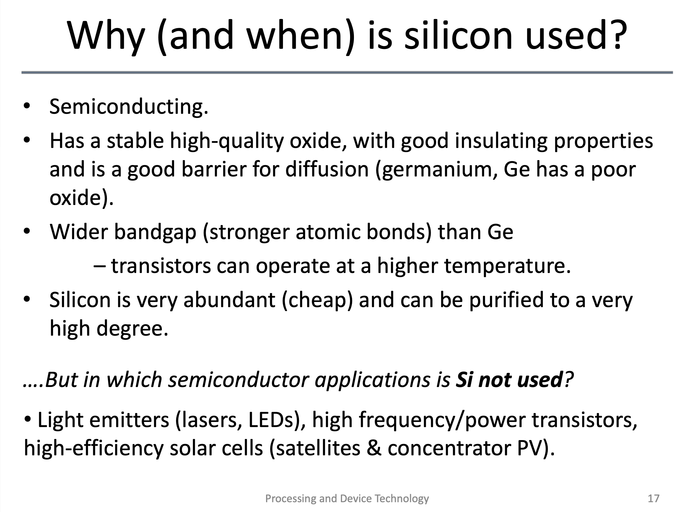
Why (and when) is silicon used?
Progress of Si technology and Moore´s law

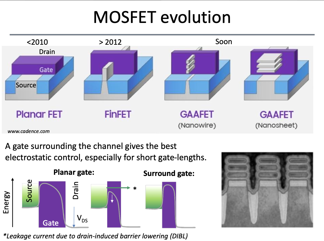
MOSFET evolution
CMOS inverter: device used for examples in course

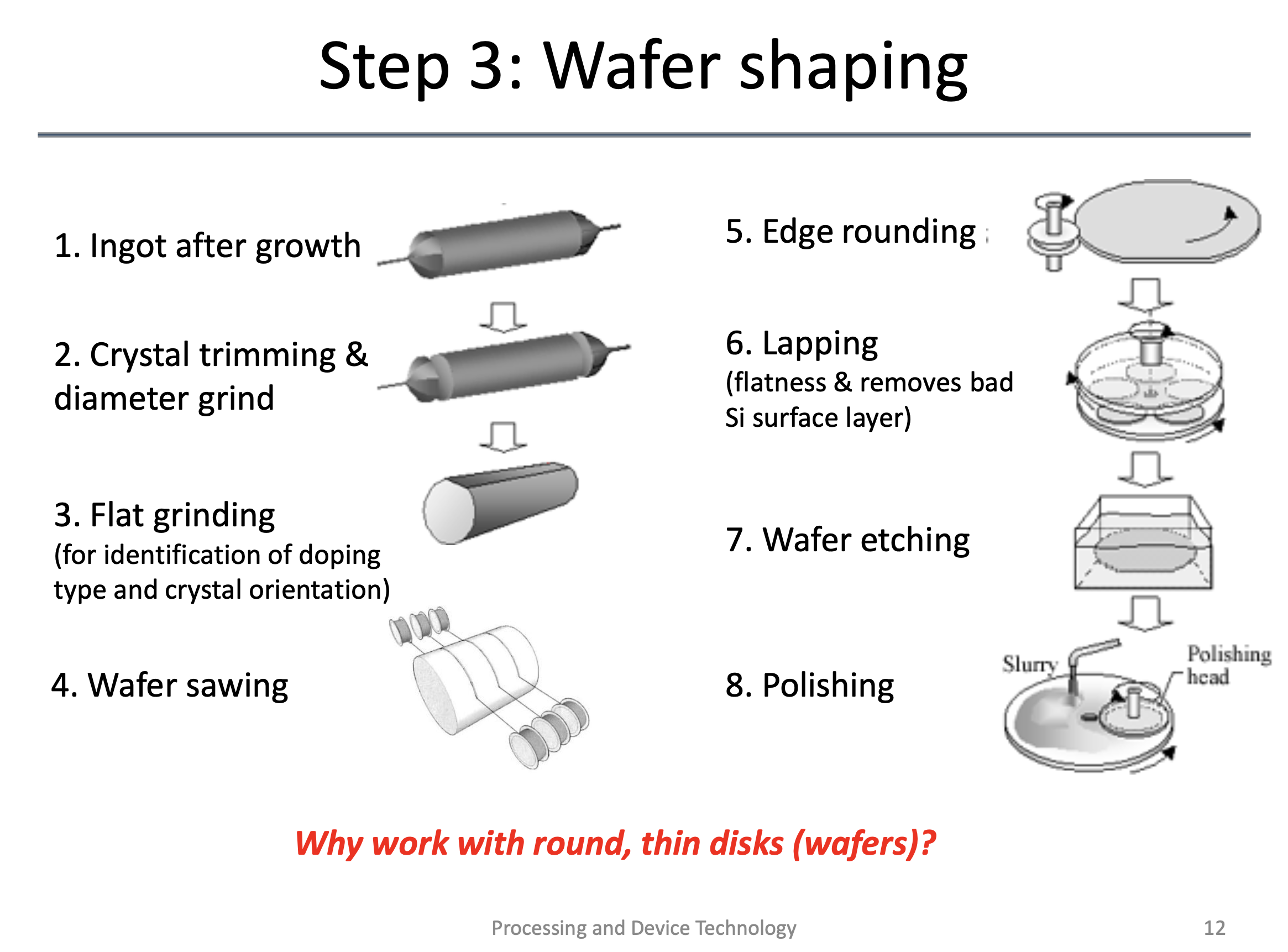
Crystal ingot to wafer process
Phase diagram (Ga-As)

Czochralski process

What determines the uptake of impurity in solid during Czochralski process

Measuring doping levels, examples

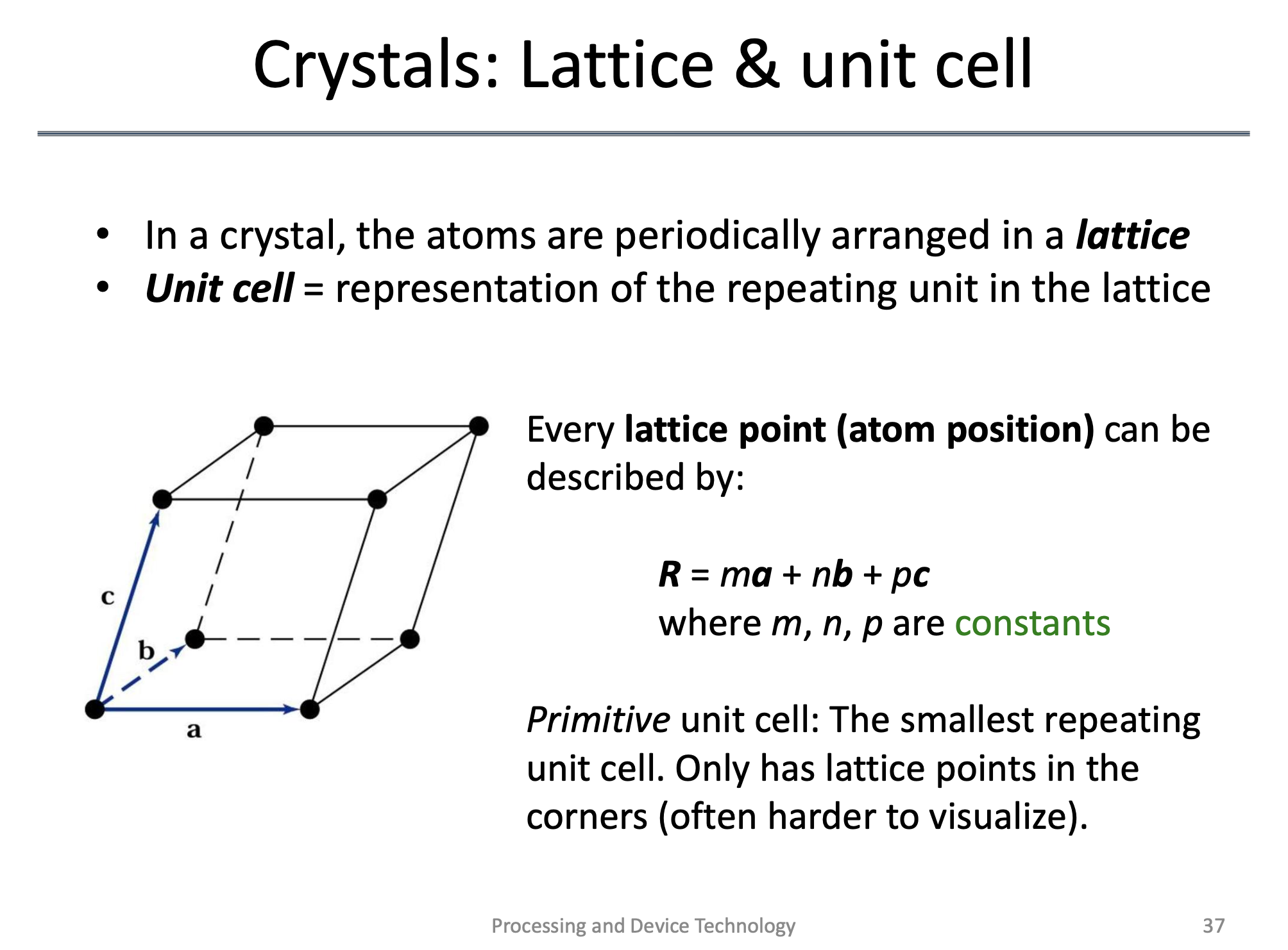
Crystals: Lattice & unit cell
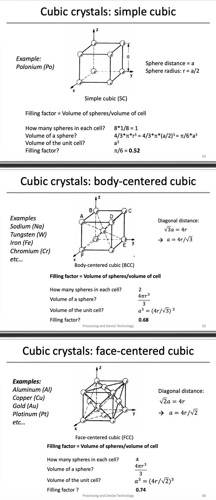
Three different cubic crystals

Crystal planes and miller indices

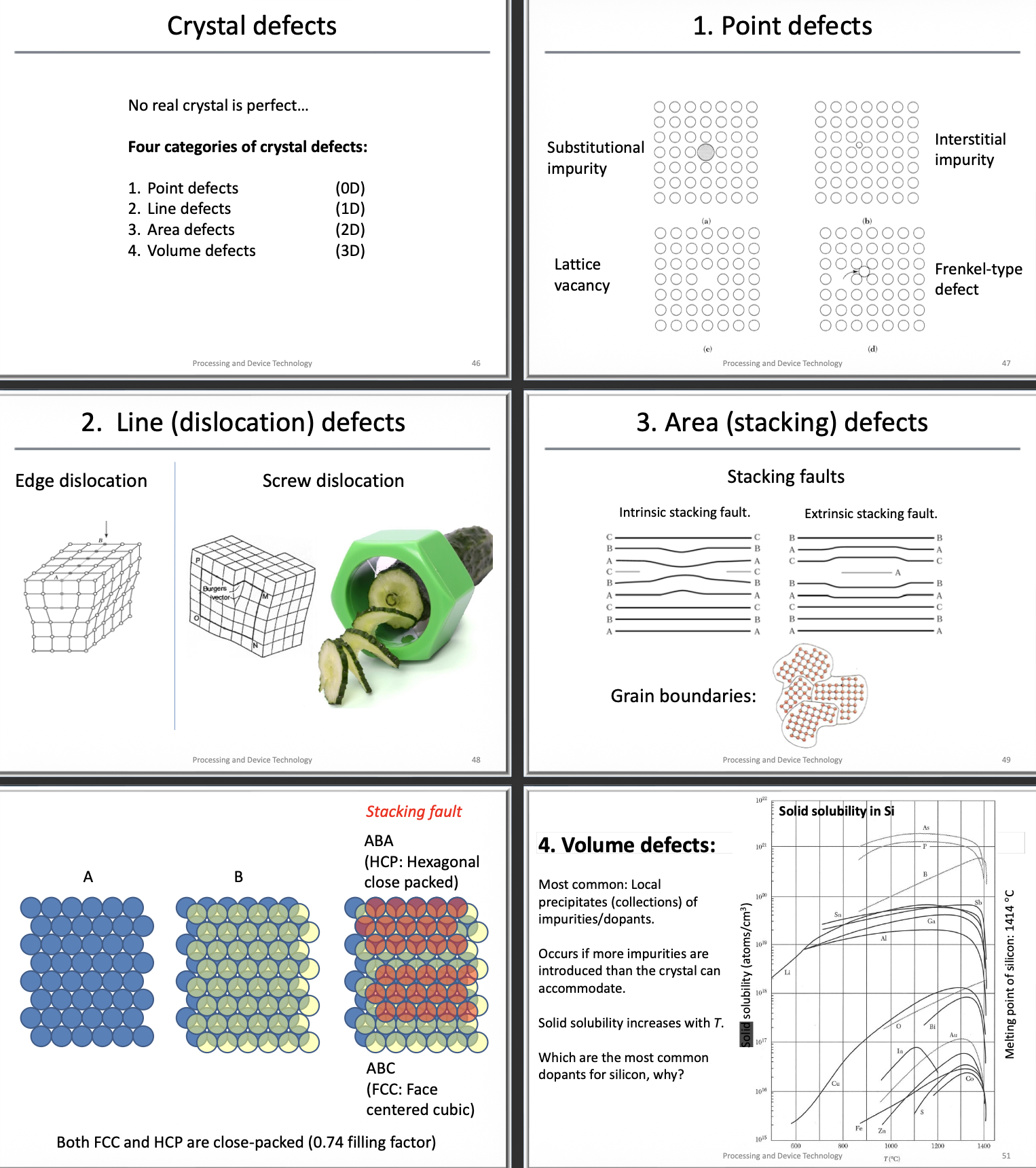
Crystal defects
Filling factor and examples of calculation for different cubic crystals
(Outside of course)
Mind map for film formation techniques
MBE – Molecular Beam Epitaxy: Atoms or molecules are directed onto a heated crystalline substrate in ultra-high vacuum, allowing highly controlled crystal growth.
LPE – Liquid Phase Epitaxy: A crystalline film grows from a supersaturated liquid solution in contact with a crystalline substrate.
VPE – Vapour Phase Epitaxy: A crystalline film grows from gaseous precursors on a crystalline substrate.
CVD – Chemical Vapour Deposition: Gaseous precursors react or decompose to form a solid film on a substrate.
PECVD – Plasma-Enhanced Chemical Vapour Deposition: Plasma activates chemical reactions, allowing deposition at lower temperatures than conventional CVD in many processes.
ALD – Atomic Layer Deposition: Alternating, self-limiting surface reactions deposit a film one atomic layer (or fraction of a layer) at a time.
PVD – Physical Vapour Deposition: Material is physically transported from a source to a substrate, typically through a vacuum.
PLD – Pulsed Laser Deposition: Short laser pulses ablate a target, producing material that deposits onto a substrate.
MO-CVD – Metal-Organic Chemical Vapour Deposition: A type of CVD that uses metal-organic precursors.
MOVPE – Metal-Organic Vapour Phase Epitaxy: Epitaxial crystal growth using metal-organic precursors in the vapour phase. It is closely related to MO-CVD, and the terms are often used interchangeably.

Various methods to form thin films in IC fabrication

Common epitaxial techniques and what semiconductors they work for

Molecular beam epitaxy (MBE)

CVD
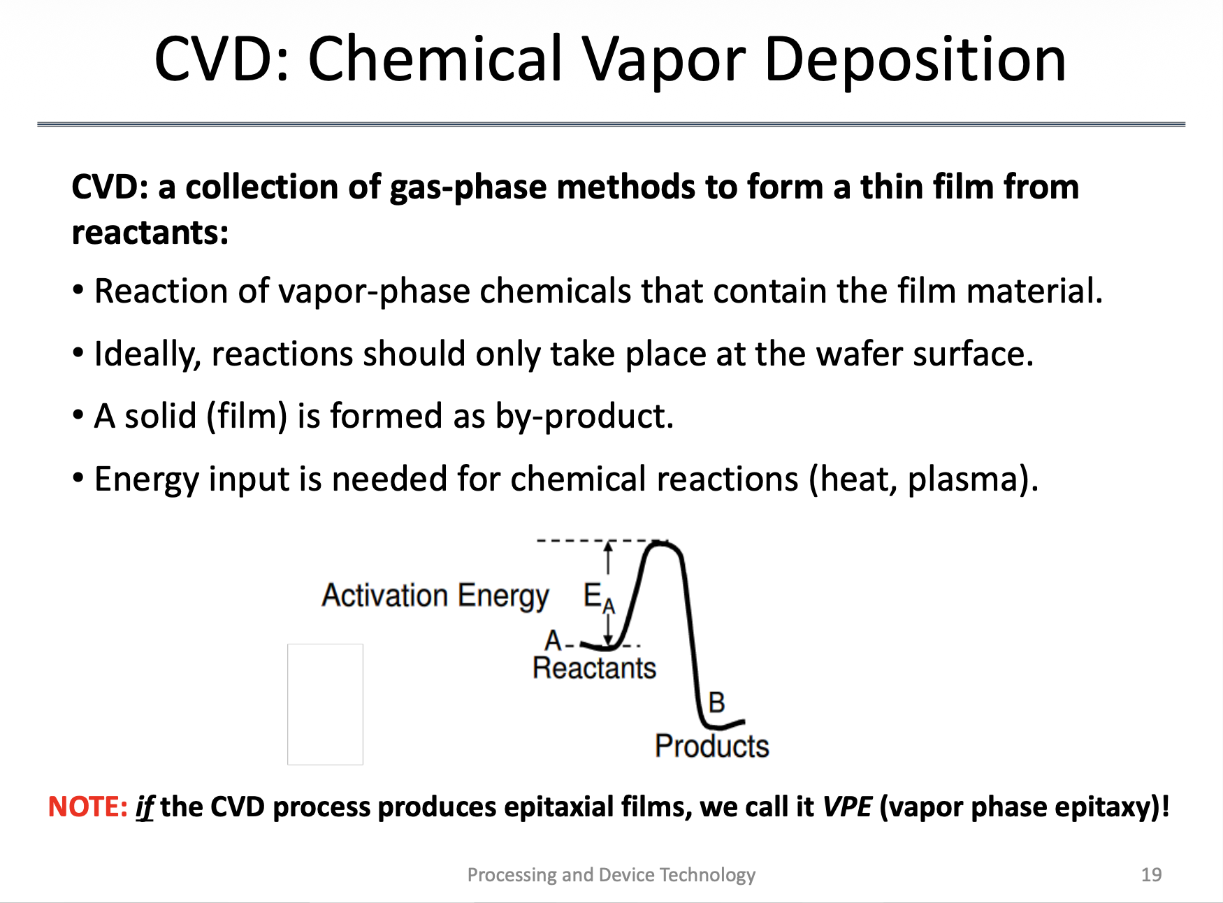
VPE

MOVPE

Goal with CVD growth, relating to how the growth should happen

Homo- and heteroepitaxy

Stranski-Krastanow island growth

III-V epitaxy on Si

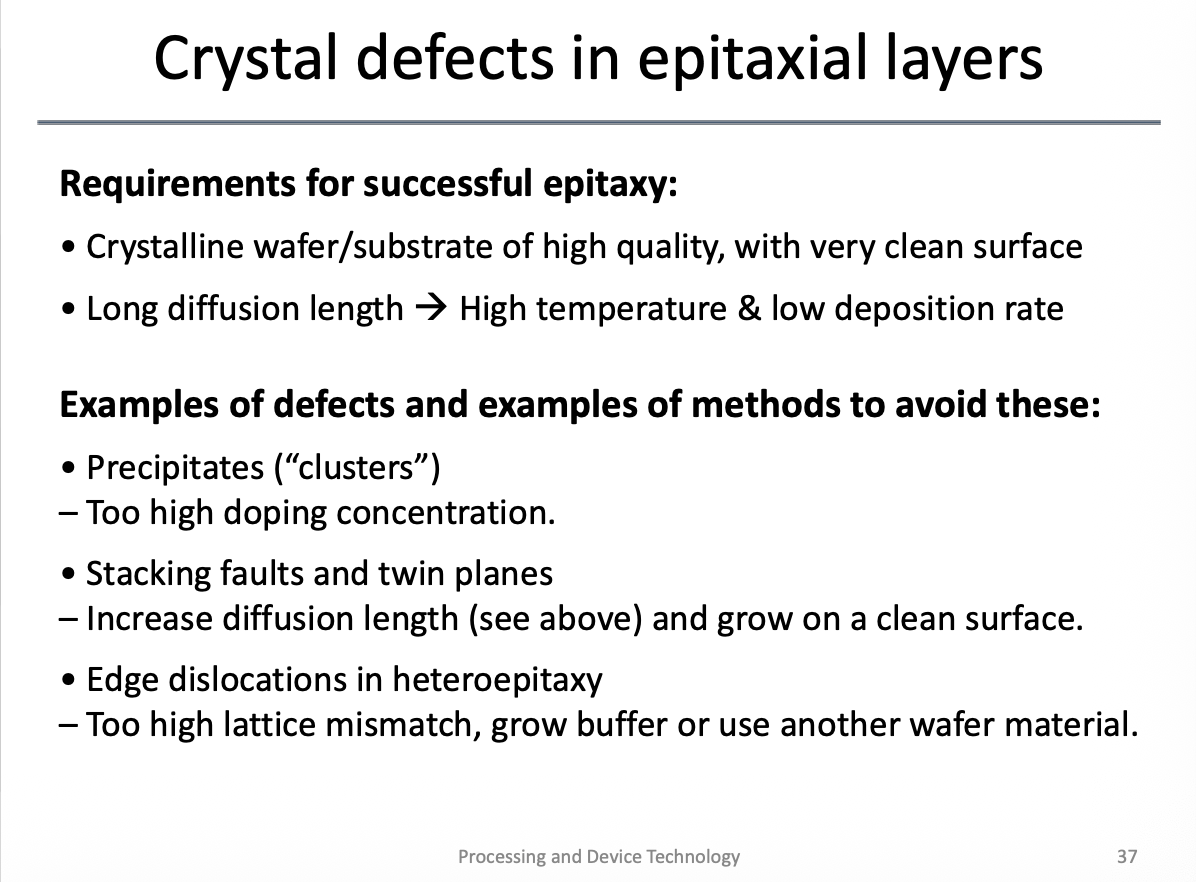
Crystal defects in epitaxial layers
Cleanrooms - general info
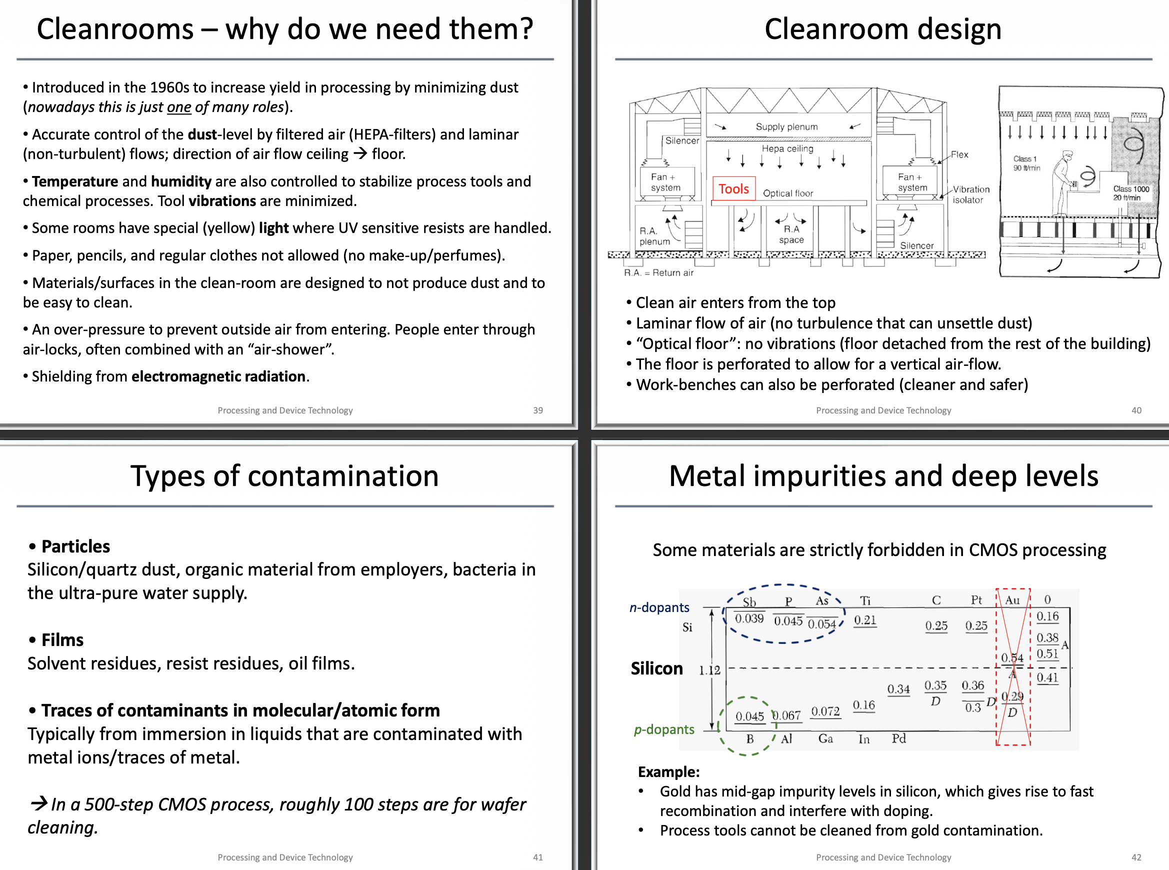
Lund Nano Lab
In industrial facilities they use “Mini-environments”: each machine has its own atmosphere and the wafers are transported in sealed boxes.

Clean room garments

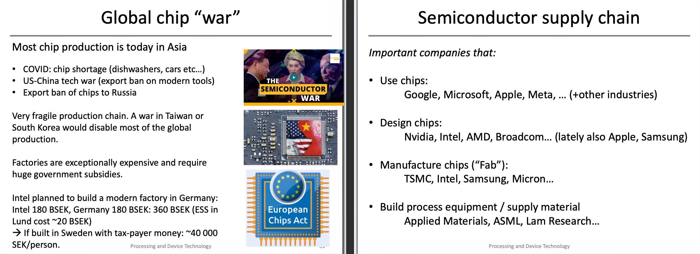
Global chip “war”
Different lithographic techniques for device processing

The photolithographic process

Priming the wafer surface

Photoresist and its types

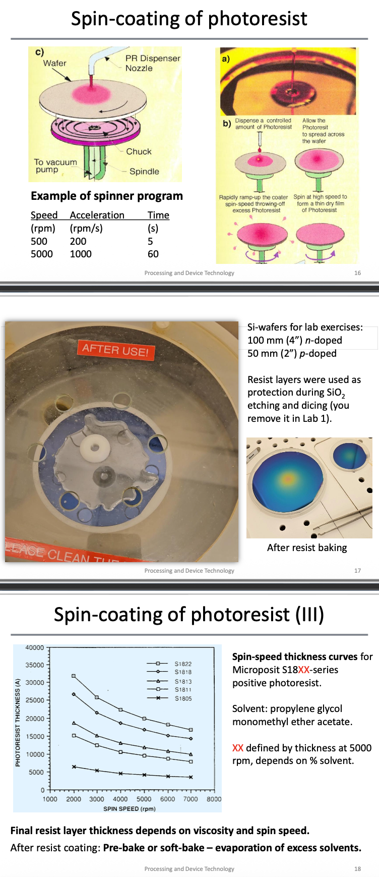
Spin coating of photoresist
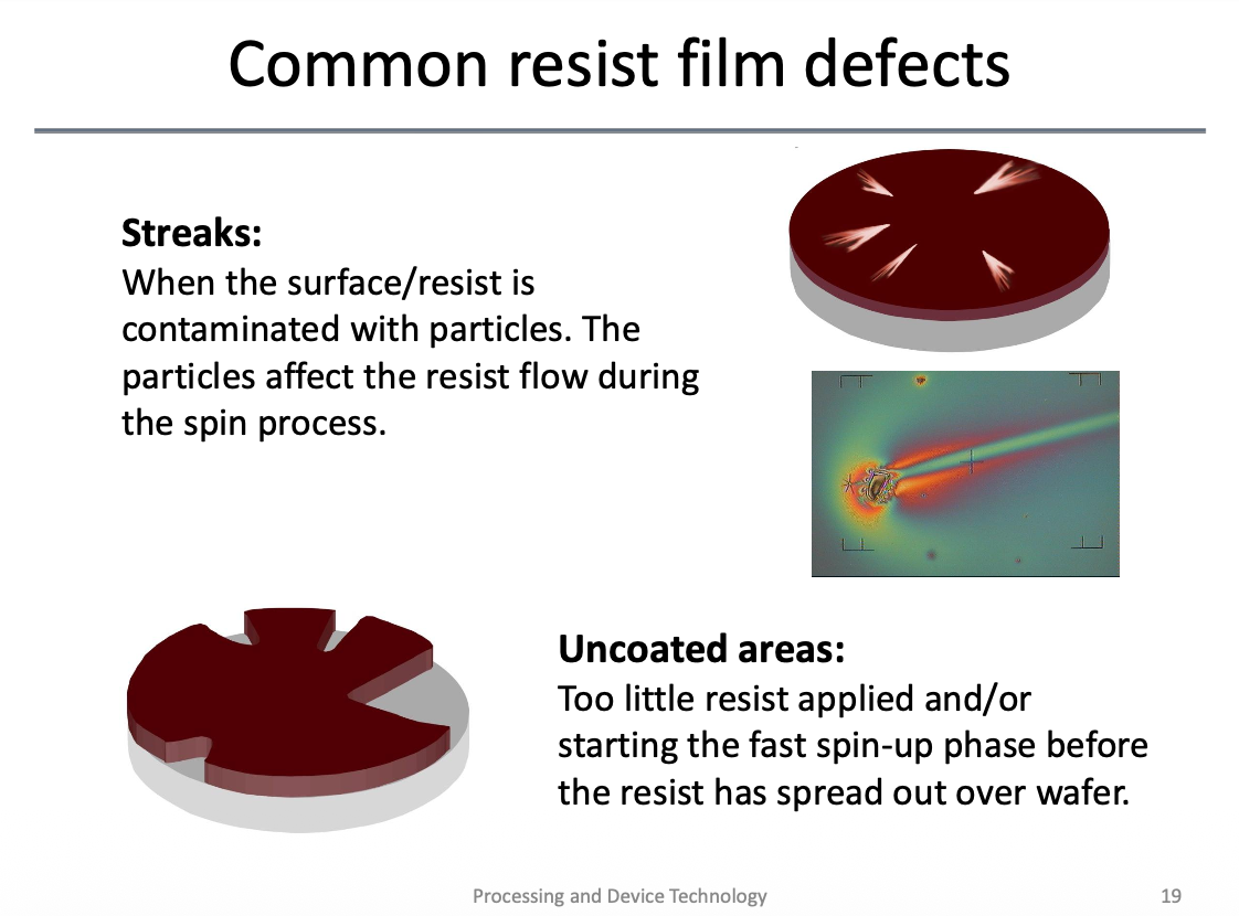
Common resist film defects
Two families of optical exposure methods

Shadow printing

Projection printing

Photomasks: Alignment and manufacturing

UV exposure tools with programmable masks

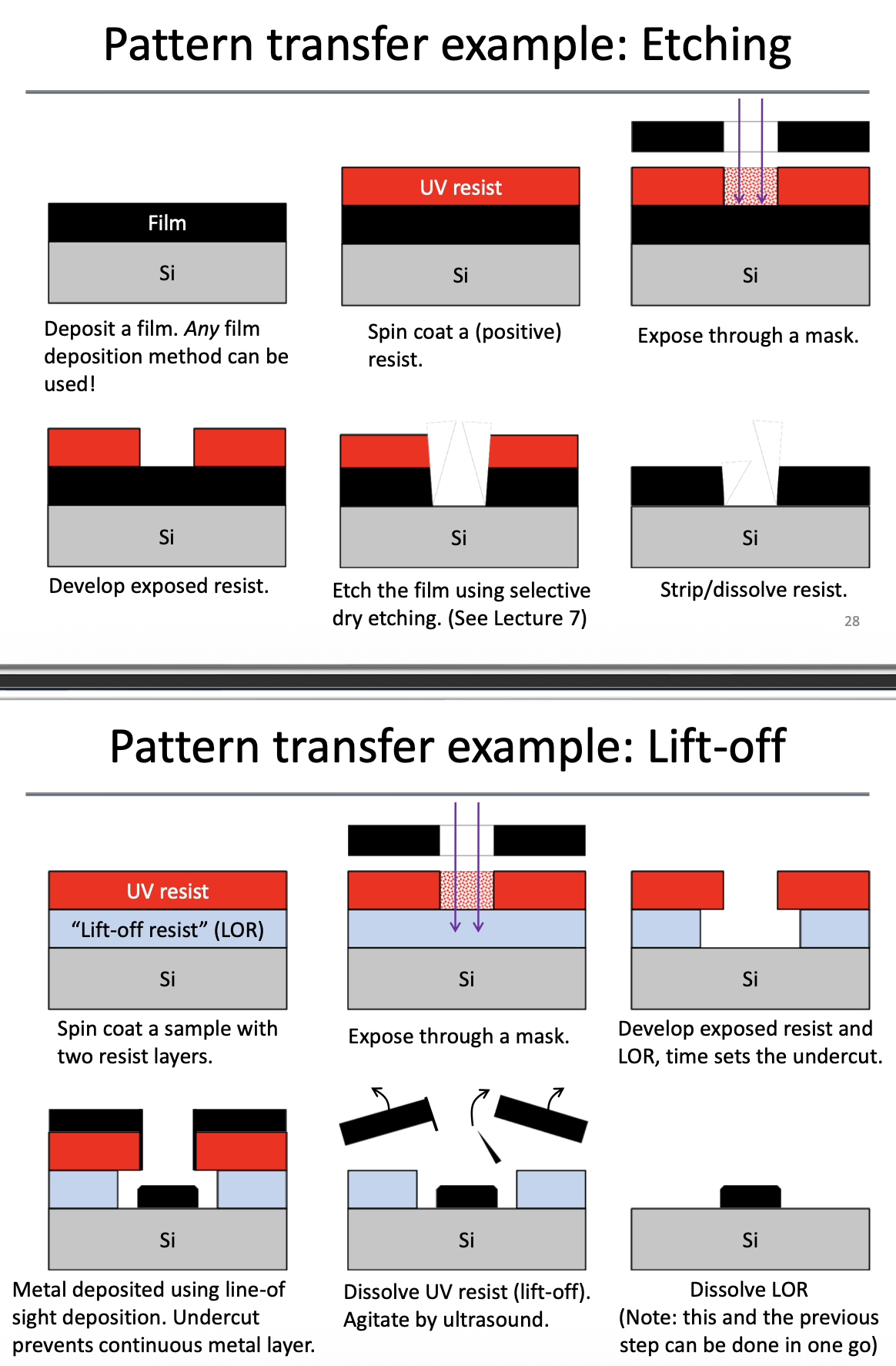
Pattern transfer example: Etching/Lift-off
Example: Multiple masking steps

Resolution enhancement techniques

Resolution enhancement techniques: Phase shift mask

Resolution enhancement techniques: Optical proximity correction (OPC)

Resolution enhancement techniques: Immersion lithography

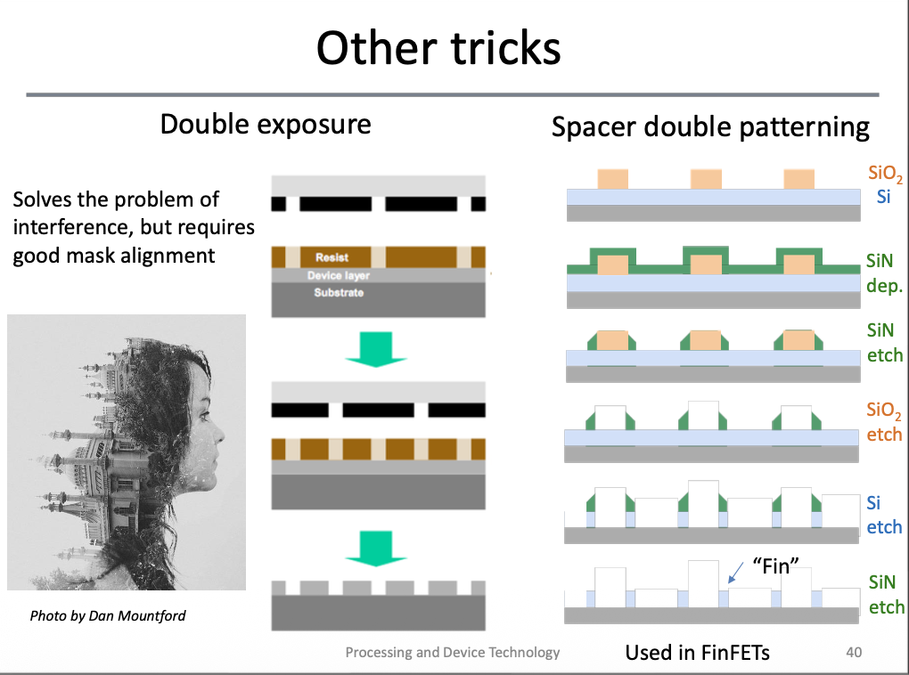
Resolution enhancement techniques: Double exposure and Spacer double patterning
Extreme-UV (EUV) Lithography

Purpose of SiO2 films and methods to form them
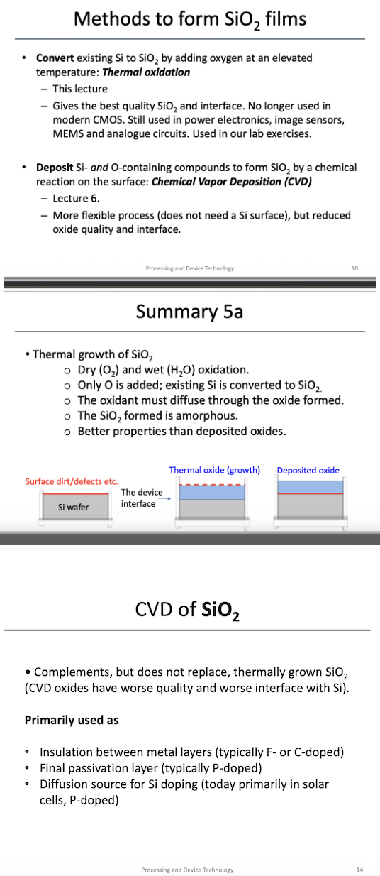
Thermal oxidation reactions
Typical oxidation temperatures: 900 – 1200 °C

Linear-parabolic model for Si oxidation

Si oxidation rate constants


Si oxidation example

How to measure thickness (e.g. SiO₂)

Measuring SiO₂ thickness from color

Interferometry and Ellipsometry
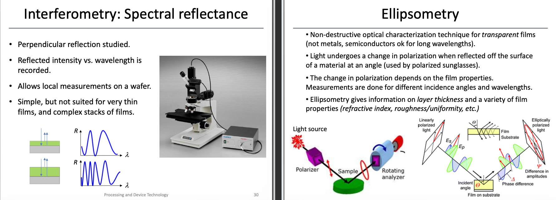
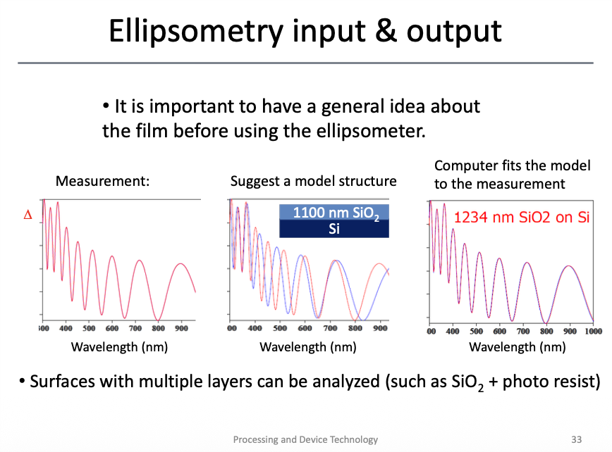
Ellipsometry input & output
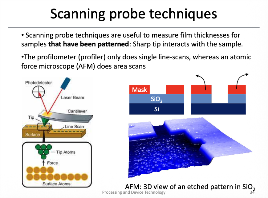
Scanning probe measurement techniques
Electrical properties of oxides and interfaces, MOS and MOSFET

nMOSFET operation

CMOS inverter logic gate and NAND logic gate

CVD: Chemical Vapor Deposition
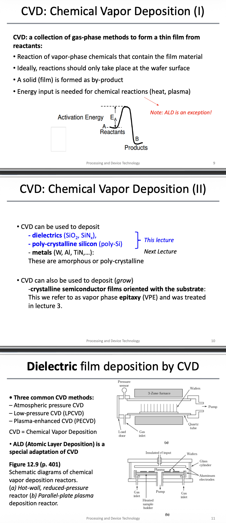
Dielectric film deposition by CVD

Plasma-enhanced CVD (PECVD)

Step coverage

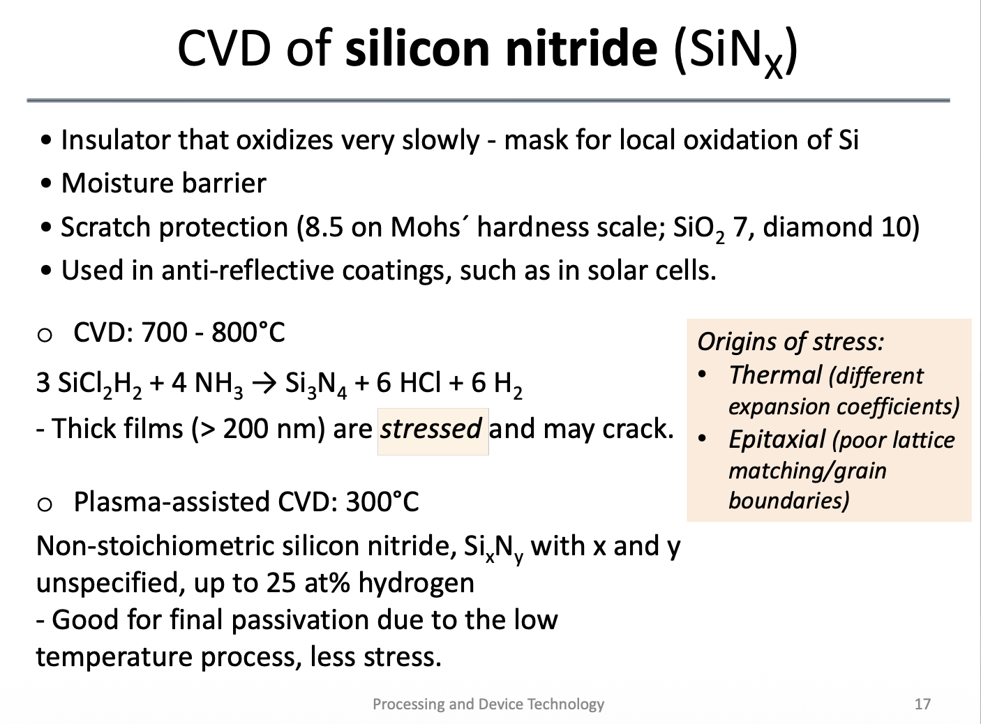
CVD of silicon nitride (SiNX)
Low-κ and high-κ dielectrics

Importance of the RC time constant

Low-κ films and example of two low-κ molecules deposited by CVD

Why we need high-κ dielectrics
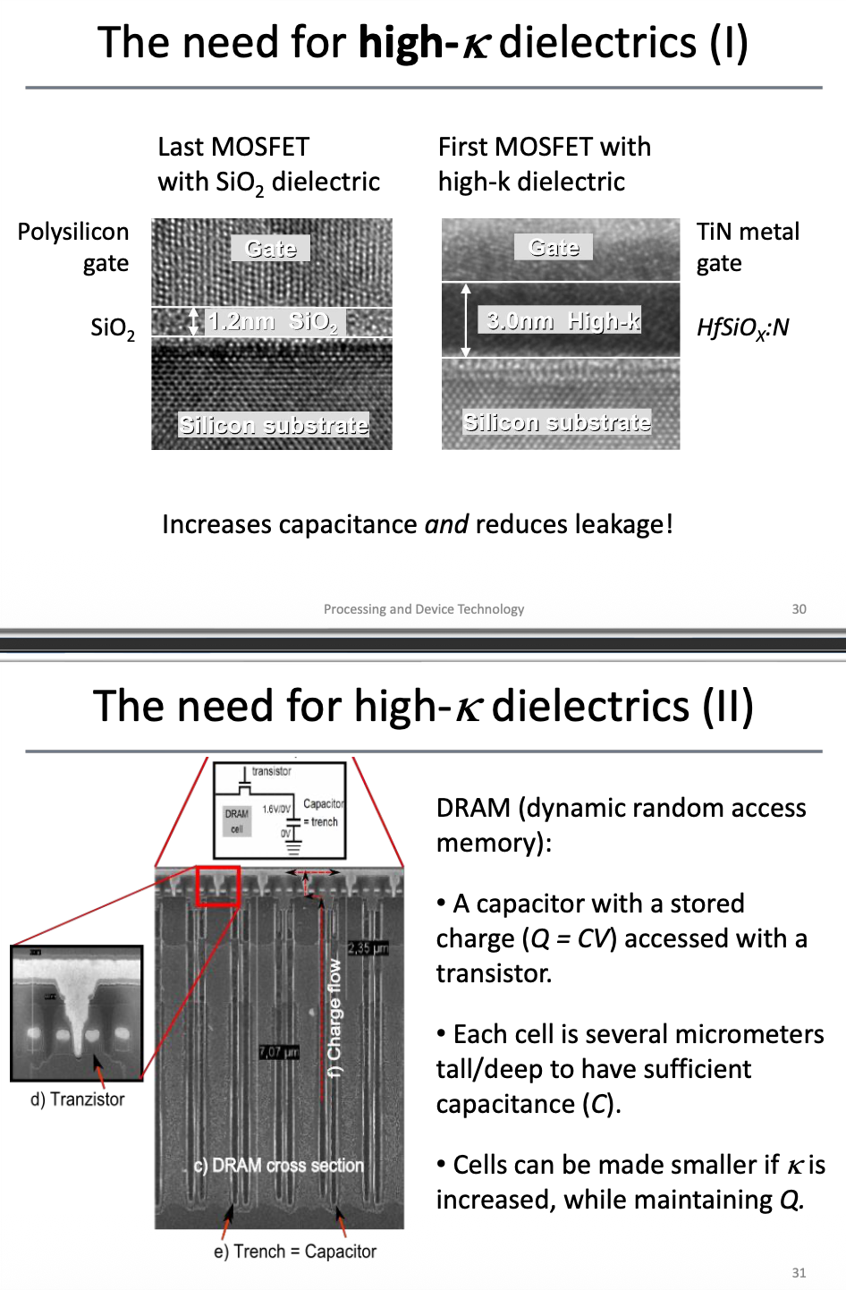
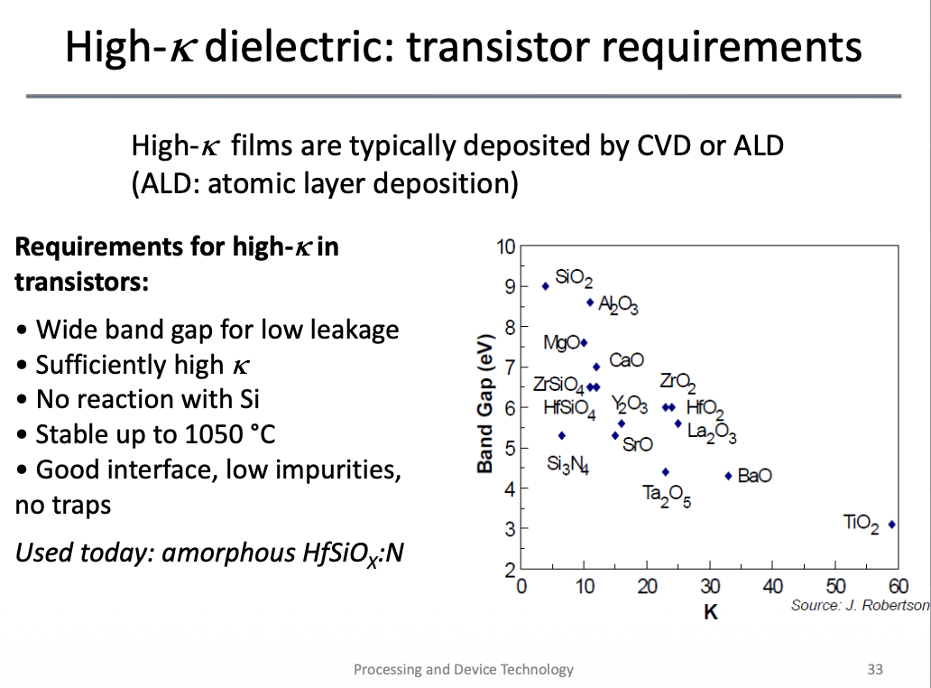
Examples of high-κ dielectrics

Requirements for high-κ in transistors
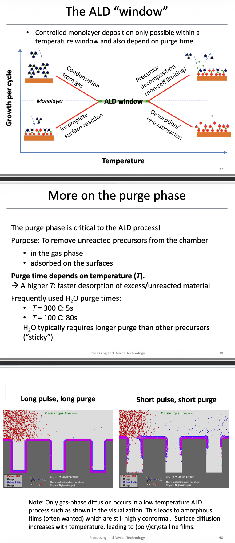
Atomic layer deposition (ALD)

The ALD “window” and the purge phase
Polysilicon films and their uses

Deposition techniques for metal films

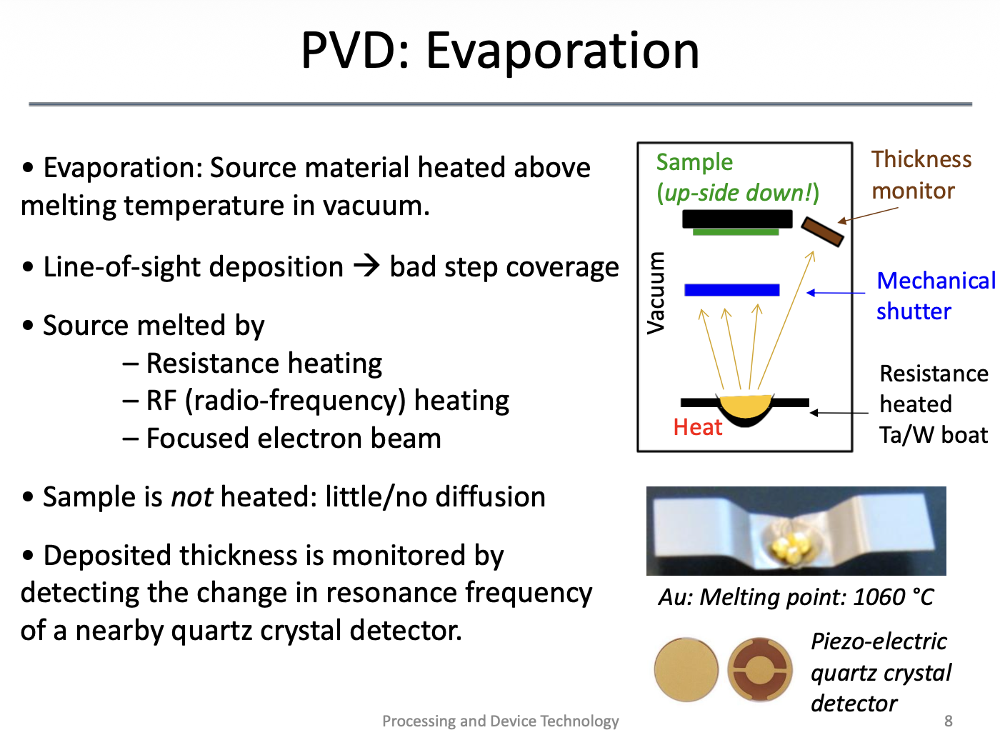
PVD: Evaporation
Pulsed laser deposition/ablation (PLD)

Sputtering and RF Sputtering
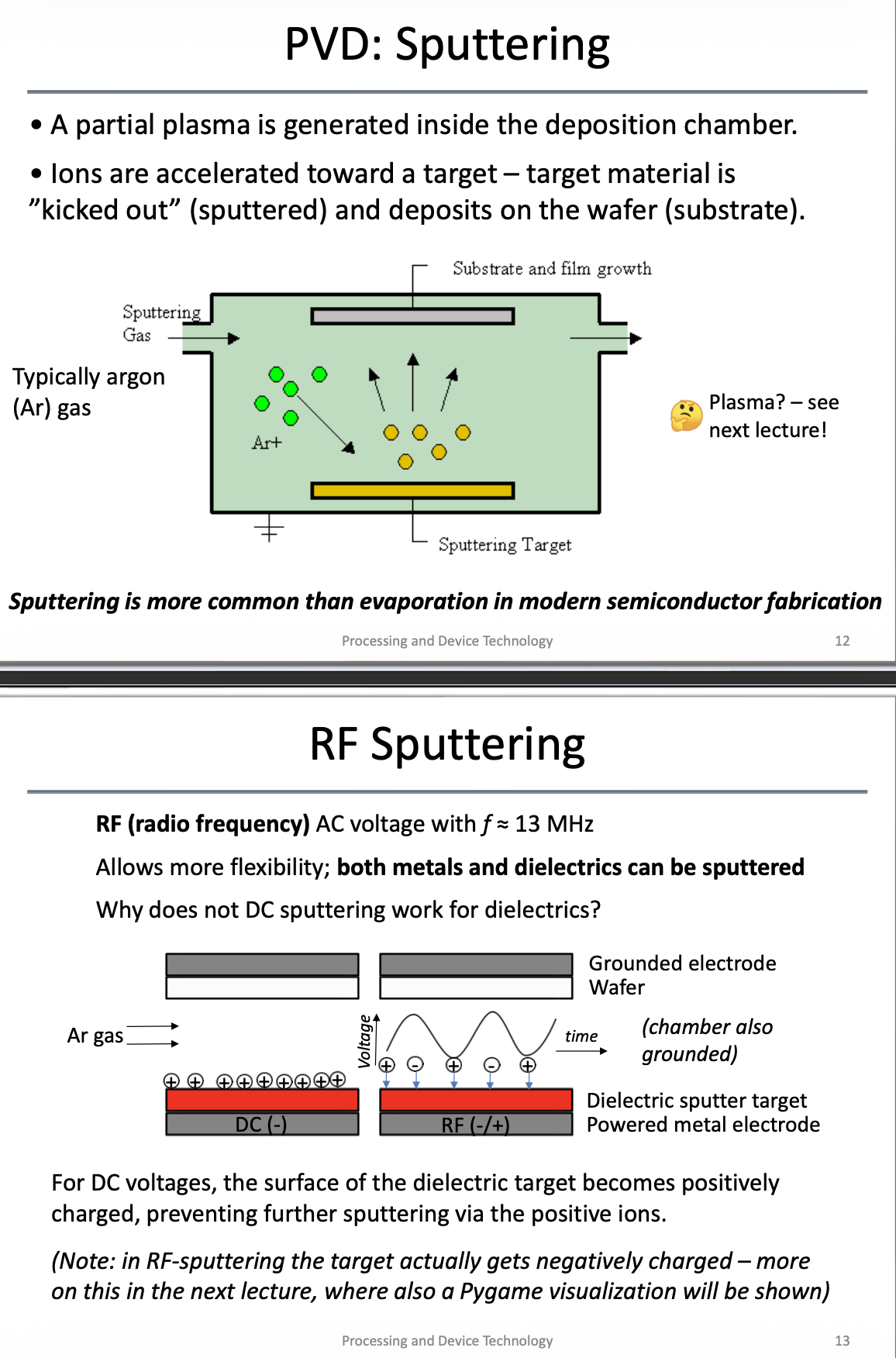
Step coverage: evaporation vs. sputtering

How an undercut limits feature density

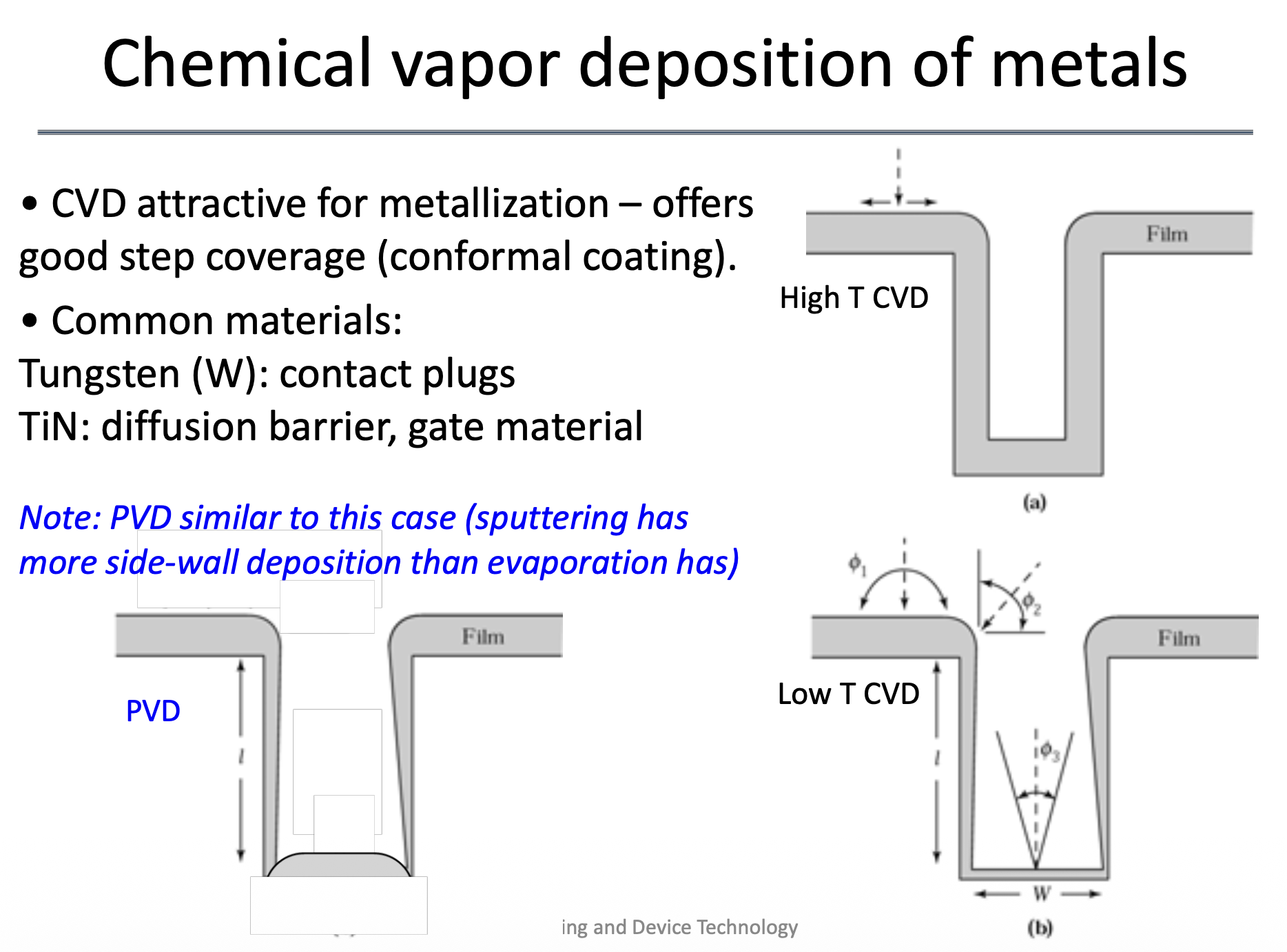
Chemical vapor deposition of metals
Silicide

Al metallization: Deposition, advantages and disadvantages

Electromigration

Cu metallization: Deposition, advantages and disadvantages

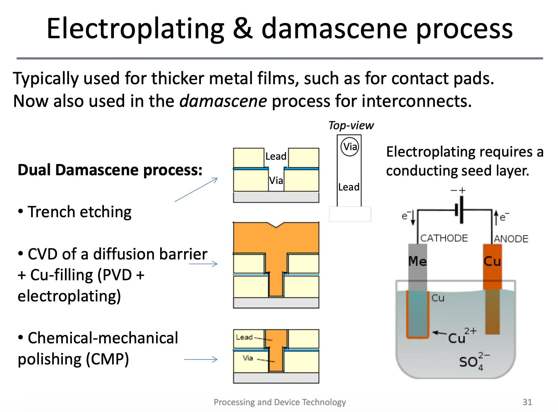
Electroplating & damascene process
Chemical mechanical polishing (CMP)

Film resistivity: Sheet resistance, RS

Electron beam lithography (EBL)

Depth comparison: Optical vs Scanning electron microscope

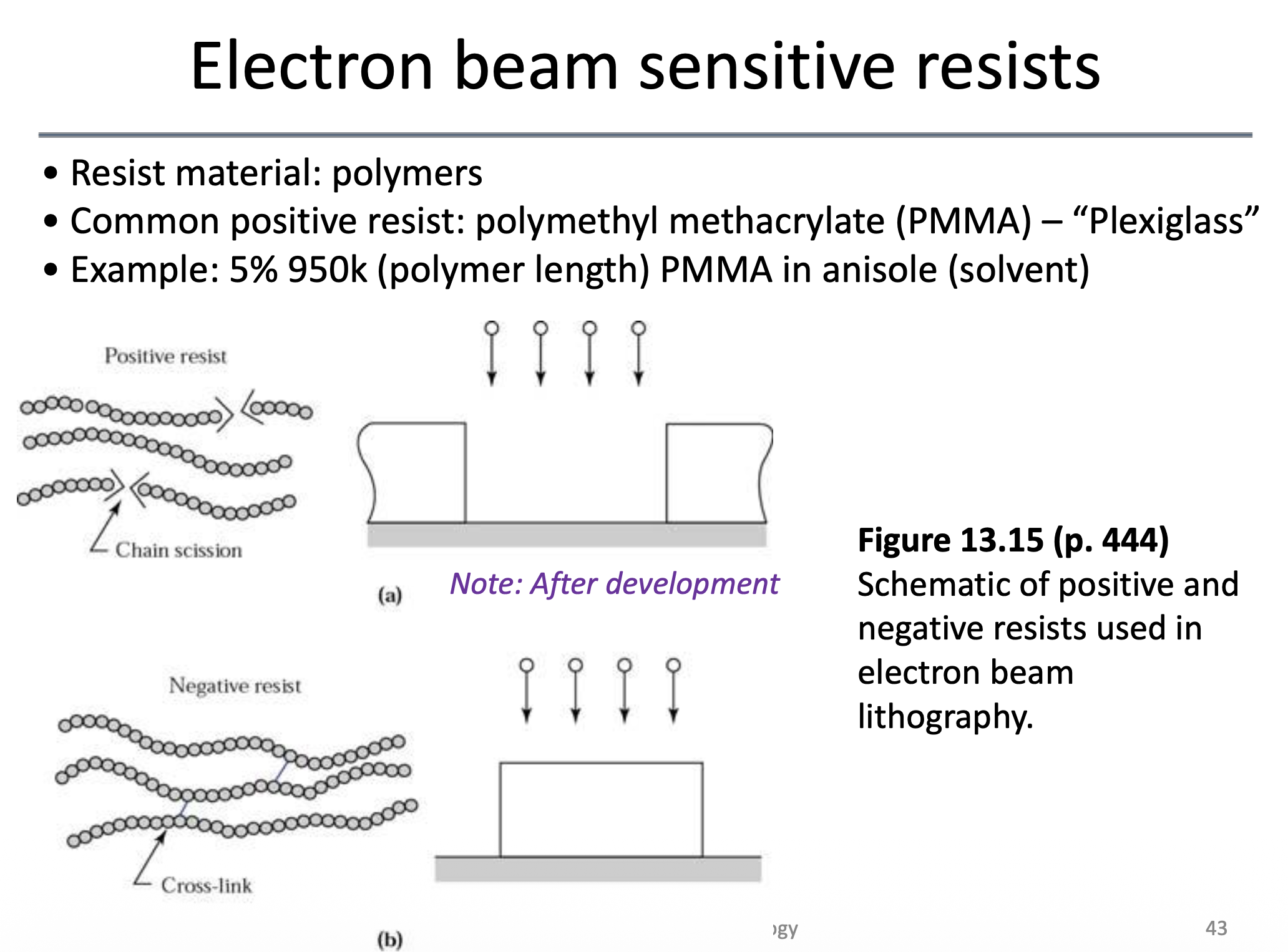
Electron beam sensitive resists: two different options
Backscattering → proximity effect

Limitation of the lift-off process

Nanoimprint lithography (NIL)

Mind map for etching techniques

Wet chemical etching
