topic 4: electrical currents
 Call Kai
 Learn
 Practice Test
 Spaced Repetition
 Match
 Flashcards
 Knowt Play
1/13

There's no tags or description
Looks like no tags are added yet.
14 Terms
filament lamp I-V graph

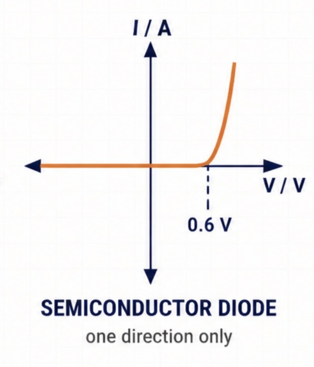
semiconductor diode I-V graph
ntc thermistor I-V graph

determining conductivity + explanation
insulator: conduction band empty ; valence band full ⇒ large band gap
semiconductor: conduction band < valence band ⇒ small band gap
an electron leaving the valence band leaves a positive hole, which appears to move the opposite way
heating a semiconductor promotes many more electrons across the gap, so band gap decreases and its resistance falls
an LDR uses light and an NTC thermistor uses heat to boost the number of conduction electrons
conductor: conduction band = valence band ⇒ no band gap
emf (of cell) definition
energy transferred (from chemical energy to electrical energy) per unit charge passing through the cell
reason for open and closing switch
opening switch between readings prevents the cell from heating up due to prolonged current flow, ensuring its internal resistance r remains constant
emf vs pd
emf: energy is transferred to electrical energy put into the circuit
pd: energy is transferred from electrical energy taken out of the circuit
ohm’s law
the current through a component is directly proportional to the pd across it, provided the temperature stays constant
investigating resistivity
METHOD
Measure diameter at 5-10 points; take the mean
Clamp the wire's left end at the ruler's zero
Attach the flying lead at 0.25 m; set 6.0 V
Record I, then switch off at once
Repeat in 0.25 m steps to the full length
REDUCING UNCERTAINTY
Average 5-10 diameters in right-angled pairs
Use small currents as resistivity depends on temperature
Switch off between readings
Use the longest wire practical
resistance without emf
Metals have a regular lattice of positive ions with free (delocalised) electrons that can move through the whole structure
Without an emf the electrons move randomly, so the average position of all the charge is stationary and there is no current
An emf sets up an electric field that pushes electrons towards the positive end. Their slow overall movement is the drift velocity
The transport equation I = nAve links current to the carrier density, the area, the drift velocity and the charge
Resistance is caused by collisions between the drifting electrons and the vibrating lattice ions, which slows the electrons down
Higher temperature means more vigorous lattice vibrations, more collisions, a lower drift velocity and therefore greater resistance
effect of temperature on carrier density
METAL
high carrier density
when heated: carrier density falls very slightly from thermal expansion ⇒ more lattice collisions ⇒ resistance rises
SEMICONDUCTOR
small carrier density
when heated (light for LDR): carrier density rises enormously as electrons gain enough energy ⇒ more electrons to conduction band ⇒ band gap decreases ⇒ extra carriers outweigh collisions ⇒ resistance falls
superconductivity
Below a critical temperature some materials show superconductivity: zero resistivity and no energy dissipated as heat
Explanation:
temperature of the material decreases the thermal energy decreases lattice ions vibrate with smaller amplitudes
when the material is cooled below its critical temperature, the lattice vibrations become so small that electrons can pass through the lattice without colliding with any ions
because there are no collisions between the conduction electrons and the lattice ions, there is no opposition to the flow of charge
Therefore, the electrical resistance drops abruptly to zero

Vout equation
V_{out}=V_{\imaginaryI n}\times\frac{R_2}{R_1+R_2}
V2V1=R2R1
internal resistance equations
Ɛ=I(R+r)
V=Ɛ−Ir
Ɛ=V+Ir