T10 - Transistors
 Call Kai
 Learn
 Practice Test
 Spaced Repetition
 Match
 Flashcards
 Knowt Play
1/63

There's no tags or description
Looks like no tags are added yet.
64 Terms
Bipolar Junction Transistor (BJT)
Acts like a current controlled current source
Metal-Oxide-Silicon Field Effect Transistor (MOSFET)
Acts like a voltage controlled current source
Transistors
Three-terminal devices that control current flow
Switch and Variable Resistor/Source
Two operating modes of a transistor
Gate, source, drain
MOSFET terminals
MOSFET Operation
Behaviour controlled by electric field (voltage) applied to gate terminal
Voltage controlled current source
Ideal MOSFET equivalent circuit

Depletion MOSFET
Has an implanted channel that conducts when VGS = 0

Enhancement MOSFET
Does not have an implanted channel, non-zero VGS required before it conducts
n-channel MOSFET
Made from a thin channel of n-type semiconductor in block of p-type semiconductor
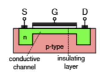
Gate-source voltage (VGS)
Controls drain current, iD
Drain-source voltage (VDS)
Drives drain current, iD
Negative gate-source voltage
Repels free electrons from channel and increases resistance
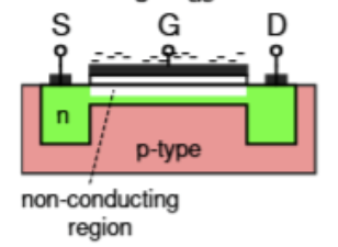
Positive gate-source voltage
Attracts free electrons to channel and decreases resistance

Low drain-source voltage
Linear (triode) region: FET acts like a resistor, iD proportional to VDS
High drain-source voltage
Pinch-off region: FET acts like constant current source, high voltage difference between gate + channel → conduction channel becomes narrow at drain end
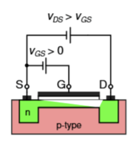
Drain current increases
n-channel MOSFET when VGS increases
Drain current decreases
p-channel MOSFET when VGS increases
Base, emitter, collector
BJT terminals
BJT Construction
Base is thin p-type material between n-type emitter and collector

Anode
p-type region
Cathode
n-type region
BJT Operation
Collector current (iC) is controlled by a smaller current into the base (iB)
NPN Transistor
Base is p-type region

PNP Transistor
Base is n-type region

NPN Transistor Operation
Base-emitter junction is forward biased + base-collector junction reversed biased. Electrons flow into the emitter but many are swept across collector instead due to thin base. Creates conventional current into the collector.
Amplification for NPN Transistor
iC = βiB
Current Gain in Transistor
β (between 10 - 1000)
NPN cutoff region
VBE ≤ 0 and VBC ≤ 0 (base-collector is reverse biased)
NPN active region
VBE > 0 and VBC ≤ 0 (base-collector is reverse biased)
NPN saturation region
VBE > 0 and VBC > 0 (base-collector is forward biased)
Acts as open switch
NPN transistor behaviour at cutoff region (iC = iB = 0)
Acts as current amplifier
NPN transistor behaviour at active region (iC = βiB)
Acts as closed switch
NPN transistor behaviour at saturation region (iC is max)
MOSFET Advantages
Easier to drive (w/ voltage), faster switching, better thermal stability, manufacturing dominance
BJT Advantages
Used for very low-noise analog front ends, precision linear amplifiers, high-volt power amplifiers, low on-state voltage/resistance
Very High
MOSFET input impedance
Low (requires biasing)
BJT input impedance
Gate-source voltage <= 0
n-channel enhancement FET acts as an open switch (iD = 0)
Gate-source voltage <= 0
n-channel enhancement FET acts as a closed switch (iD > 0)
Gate-source voltage >= 0
p-channel enhancement FET acts as an open switch (iD = 0)
Gate-source voltage < 0
p-channel enhancement FET acts as a closed switch (iD > 0)
Pulse Width Modulation (PWM)
Applying a pulsed voltage to a DC motor via transistors acting as switches

PWM Operation
Mechanical interia keeps motor spinning between pulses and windings have inductance → keeps current/torque flowing
Duty Cycle
% of time that voltage is high for PWM
H-Bridge
Uses 4 switches (transistors) to provide variable speed and direction of rotation

A and B, C and D
H-bridge switch couples (typically turn on/off together)
Forward Rotation
A and B on (VM = VS)

Reverse Rotation
C and D on (VM = -VS)


H-Bridge Diodes
Protect transistors so current from inductance flows back into source VS and not into transistors
MOSFET Characteristic
Linear and pinch-off regions

MOSFET Ideal Linear Model
Just pinch-off regions

Equivalent Model of MOSFET in pinch-off

Ideal MOSFET Model Assumptions
Gate terminal is open circuit (very high impedance), drain current proportional to VGS
Transconductance
gm, constant and measured in Siemens, S
Drain current when gate-source voltage = 0
ID0
Common Source Amplifier
Single transistor amplifier with large negative gain (inverting)
Common Source Amplifier Circuit

Increase R1
Increase gain in common source amplifier circuit
Voltage Range of Common Source Amplifier
0 ≤ Vout < VDD
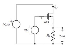
Source Follower Amplifier
Single transistor amplifier with gain between 0 and 1 (non-inverting power amplifier)
Source Follower Amplifier Circuit

Load Line
Relationship imposed on VDS and iD by circuit external to transistor
Operating Point
Where load line intersects the FET characteristic (both must be satisfied simultaneously)
