MEMS Final
Applications of MEMS devices = drug delivery, DNA microarray, lab on a chip, neural probe
scaling laws = deal with structural and functional consequences of changes in size or scale among otherwise similar structures/organisms
Scaling in geometry:
surface area = A~l²
volume = V~l³
Energy required to heat a system to temperature T~l³
strength~l²
weight~l³
inertia=mr²~l³*l²
Heat loss ~ l²: as animals get smaller, a greater percentage of their energy intake is required to balance heat loss
A/V~l²/l³ = 1/l: As l decreases A/V related forces/phenomenon becomes more important
Two types of phenomena:
with higher power >l² dependencies there is a reduced effect at smaller size scales
with lower power <l² dependencies there is an increased effect at smaller sizes
Liquid evaporation in biosensors becomes an issue due to scaling laws
MEMS materials = silicon (single crystal, polycrystalline) - well established fab methods, easy to integrate electronics, poor biocompatibility, lack of optical clarity; most commonly used semiconductor, abundant and can be grown as very pure large crystal, can be doped to add electrons or holes as conductors, metals (aluminum, copper, gold, titanium, platinum), insulators (silicon dioxide, silicon nitride, titanium nitride)
MEMS processes = lithography, etching, deposition, packaging
Intrinsic Conductivity = increasing T causes production of free carriers, equation: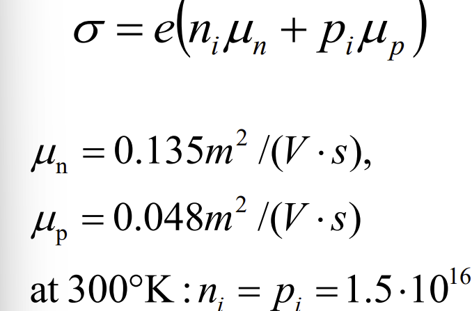 N-type doping = small amount of Si replaced with group V element, extra electron for each atom replaced, negative charge carrier
P-type doping = small amount of Si replaced with group III element, hole created for each atom replaced, positive charge carrier
Extrinsic semiconductors = dopant concentration is 5 to 6 orders of magnitude higher concentrations than the intrinsic conductors in silicon, conduction primarily by impurity carrier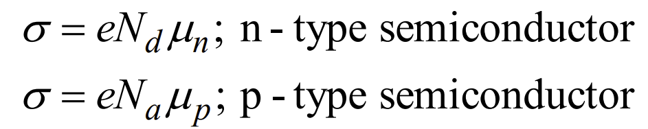 p-n junction = where n-type and p-type semiconductors meet
diode = one way valve for current flow
Light emitting diode (LED) = p-n junction that emits light when activated, color determined by energy band gap
electroluminescence = when electrons and holes recombine, energy is released in the form of photons
Transistors = switch and amplify, central to integrated circuit, bipolar junction transistor
field effect transistors = 3 terminals, gate (conductor), source and drain (highly doped same type semiconductor), used in most computer systems
integrated circuits (IC) = complete circuits on single chip consisting of active (diodes, transistors) and passive (resistors, capacitors, inductors) components
Moore’s Law = number of transistors on a chip doubles every 2 years
microfabrication processes = property modification (diffusion → ion implant), patterning (lithography), subtractive processes (wet/dry etching), additive processes (oxidation, physical vapor deposition, chemical vapor deposition), packaging
Czochralski method = Si crystal growth, molten Si bath seed pulled at 2-5 cm
wafer slicing = slice ingot using diamond saw, polish surface, sort
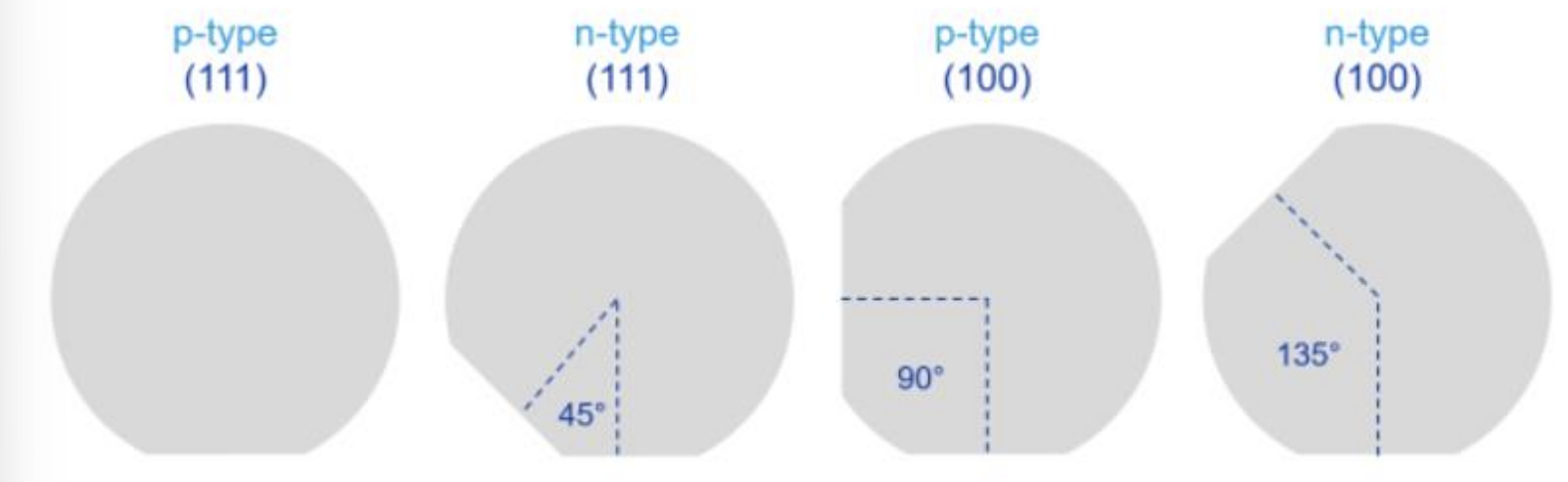
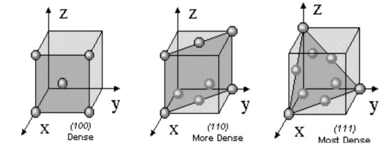
Si wafer orientation:
 Polycrystalline silicon = thermally grown or deposited films, similar mechanical and chemical properties as single crystal Si, usually used as structure material
silicon dioxide = thin silicon dioxide film formed on silicon exposed to oxidizing ambient, thicker oxide films are thermally grown or vapor deposited and are amorphous, used for surface passivation, readily dissolved in HF → used as sacrificial layer
silicon nitride = vapor deposited amorphous film, structural material, diffusion barrier against moisture and sodium, surface passivation, etch mask
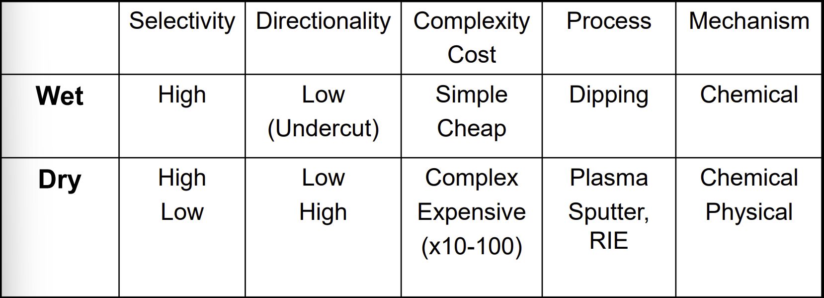
etching = subtractive process, wet etching = chemical solution, dry etching = plasma, reactive ion or sputter, issues = directionality and selectivity, masks for each surface = photoresist, oxide/nitride
etching profiles = isotropic (same rate in all direction, wet: etch rate may be fast, masks are undercut, high aspect ratio difficult because of diffusion limits, stirring enhances isotropy), anisotropic (crystal plane dependent, wet: usually in alkaline solutions (KOH, TMAH), heating typically required for rate control, etch rate dependent on crystal direction, etch mask = SiO2 (short term), SixNy (excellent), Si with heavily doped P as etch stop, thermal inkjet printhead, etomic force microscopy tip)
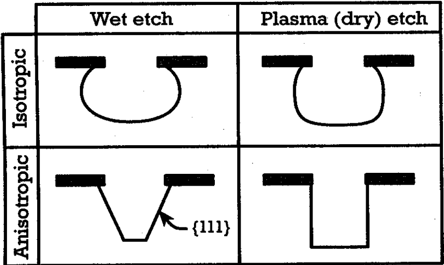
 dry etching = physical bombardment (ion mill, physical sputtering), plasma etching (plasma assisted chemical etching), reaction ion etching (chemical reaction + ion bombardment)
Deep reactive ion etching (DRIE) = alternating reactive ion etching and polymer deposition, high aspect ratio etching
 Deposition = physical vapor (materials transported in vapor form from source to substrate through vacuum or low pressure gaseous environment - evaporation, sputtering), chemical vapor (deposition of solid on a substrate from chemical reaction in vapor phase, film growth from vapor/gas phase via chemical reactions in gas and at substrate)
Evaporation = high vacuum, line of sight deposition, poor step coverage, low surface damage
sputtering = low-medium pressure, good step coverage and adhesion, ion bombardment damage, possibility of incorporating impurities
substrate bonding methods = silicon direct bonding, silicon to silicon fusion, anodic bonding, adhesives, laser bonding; prerequisites = clean and flat surfaces; issues = difference in coefficient of thermal expansion
Packaging = high cost, considerations - biocompatibility, cleanroom accessibility, expiration date, hermetic sealing, mechanical stress, implantability, power systems etc., basic approaches - monolithic integration, multi-chip module, integrating multiple subsystems
example process flow = silicon substrate → metal deposition → photolithography → metal etching → resist removal
two primary techniques for patterning additive and subtractive processes = etch back (photoresist is applied overtop of layer to be patterned, unwanted material is etched away), lift off (patterned layer is deposited over top of photoresist, unwanted material is lifted off when resist is removed)
etch-back process = deposit thin film of desired material → coat and pattern photoresist -. etch film using photoresist as mask → remove photoresist
lift off process = coat and pattern photoresist → deposit thin film of desired material → swell photoresist with a solvent → remove photoresist and thin film above it
pressure sensor = Si → nitride film deposition → photolithography → nitride etching → KOH etching
Polymer MEMS:
advantages = versatility of material composition and properties, biocompatibility, good optical transparency, ability of enclose high aspect ratio structure, simple and low cost fabrication, more accessible to chemists/biologists
disadvantages = low thermal stability, low thermal and electrical conductivity, incompatible with organic solvents
types used in MEMS = elastomers (polydimethylsiloxane PDMS), thermoplastics (polymethylmethacrylate PMMA, polycarbonate PC, polystyrene PS), hydrogels (smart hydrogels, polyethylene glycol PEG, polyvinyl alcohol PVA), biodegradable polymers
PDMS = watertight, gas permeability, low toxicity, transparency, self seal by conformal contact, simpler and less expensive fabrication procedure, chemically modifiable
Thermoplastics = high optical clarity, PMMA is economic alternative to PC, molding to create microfluidic channels
SU-8 = negative photoresist, high aspect ratio structure, highly resistant to solvents, acids, and bases, high temperature stability
Hydrogels = water-swollen crosslinked polymers, photopolymerization, volume change in response to external stimuli (pH, temp, electrical field etc.)
Biodegradable polymers = important for drug delivery and tissue engineering, early stage of research, molding, embossing, soft lithography
Polymer Microfabrication = soft lithography, molding (injection, compression, hot embossing), rapid prototyping
Soft Lithography = collection of fabrication methods that are all based on using a patterned layer of elastomer (PDMS)
Microcontact printing = printing on planar surface with planar/rolling stamp, printing on non-planar surface with a planar stamp
Replica molding REM = PDMS → mold polyurethane → cure PU, peel off → PU
Micromolding in capillary = use capillary force to fill gap between substrate and PDMS mold (PDMS mold → place prepolymer at one end → fill channels by capillary action → cure, remove mold)
Solvent assisted microcontact molding = uses a solvent to wet PDMS mold and soften the support polymer, dissipate and evaporate solvent through PDMS (PDMS → place mold on support → evaporate solvent → remove mold)
Soft lithography:
advantages = convenient, low cost, rapid prototyping, deformation of PDMS provides route to complex patterns, no optical diffraction limit, non-planar or curved surfaces, generation of 3D u-structures, control over surface chemistry, broad range of materials, applicable to manufacturing, patterning over large areas
disadvantages = distortion of patterns, poor registration/alignment, compatibility with IC processes, defects and their densities, uCP can only be applied to a number of surfaces, MIMIC is relatively slow process
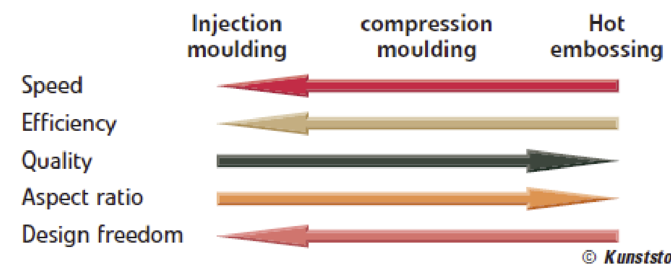
Injection molding = thermoplastics and some elastomers, liquefied materials pushed into a closed die, hardens into a shape defined by the die cavity
Compression molding = mostly for thermosets, charge (powders, pellets, liquid or preform) loaded, compressed and ejected
Hot embossing = formation of surface features in polymers and glass, press a patterned master into substrate heated above Tg, two main parameters in substrate selection (PMMA and PC usually) - Tg, alpha, master for polymer substrates = Ni, Cu, Si, SU-8, PDMS
 Glass types = quartz (mined naturally or synthesized in large long faceted crystals, piezoelectric), pyrex (borosilicate glass, coefficient of thermal expansion similar to Si)
Glass properties = excellent thermal shock resistance, optical transmission properties from ultra violet to infra red, good chemical resistance, excellent electrical insulator
Glass BioMEMS = transparent, high machine cost (drilling → etching → bonding)
Glass MEMS = DNA microarray, point of care diagnostics
Glass microfabrication = photolithography (same as Si-based MEMS devices), etching (most using specialized tools, HF isotropic etching, powder blasting, ultrasonic machining, laser machining)
Powder blasting = alumina sharp particles, iron mask for selective etching, high etching rate, good control of etching profile
Ultrasonic machining = sonotrode vibrates with high frequencies and hammers abrasive particles into workpiece
Laser microfabrication = focus laser beam on glass, high power density in focal spot, plasma generation to destroy atomic lattices, high spatial resolution, access to bulk materials without mechanical or chemical contact
carbon allotropes = hybridization of atomic orbitals dictates structure of carbon materials, therefore properties
carbon MEMS = photoresists patterned and pyrolyzed in an inert environment to yield carbon films and 3D microstructures, batteries, fuel cells, electrochemical sensors
Diamond synthesis = thermodynamically less stable than graphite at room temp, high temp high pressure process, CVD more commercially viable process
diamond patterning:
oxidation → coating diamond-powder-mixed photoresist → photoresist patterning → etching of SiO2 → diamond growth → releasing of diamond structures
oxidation → SiO2 patterning → diamond nucleation → slight etching of SiO2 → diamond growth → removal of SiO2 mask
diamond MEMS = encapsulation for implants, field emitters, biosensors
microfluidics = precise control and manipulation of very small fluid flows on the order of nanoliters
microfluidics design considerations = scaling of fluidic systems, fluid mechanics (laminar flow, surface tension, diffusion, poiseuille flow
reynold’s number:
Re=PDV/u
P = density, D = hydraulic diameter, V=velocity, u=viscosity
Re<2100, laminar
Re>4000, turbulent
Re<1, creeping
Surface tensoin and capillary forces:
gravity force = capillary force
H=(2Vcostheta)/Pgr
Thermocapillary effect - maragoni flow = viscosity and surface tension decrease with increase temperature, noncontact manipulation of droplets
electrowetting = externally added electrostatic charge modifies surface tension
poiseuille flow = steady incompressible laminar flow through a tube of constant cross section driven by pressure difference
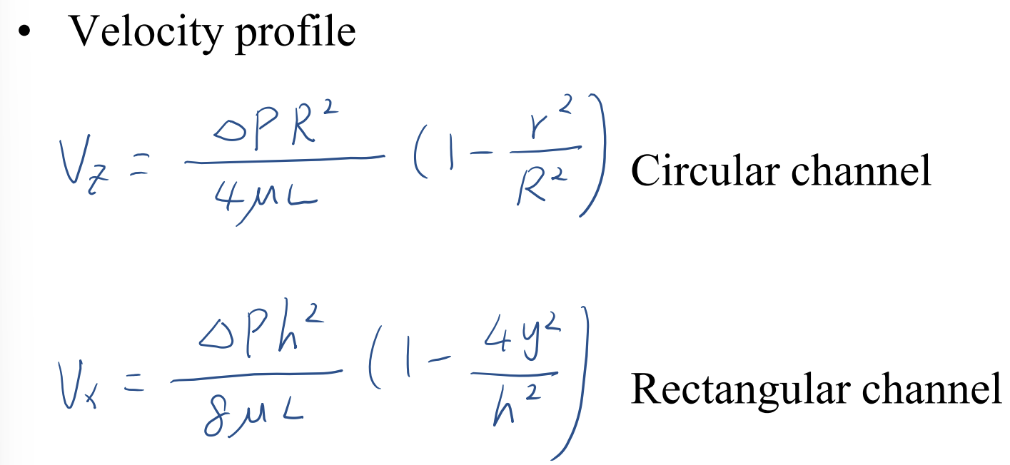
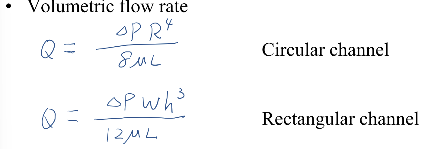 Pressure-driven flow rect channel = change P/(12uL/Wh³), flow rate = I, pressure difference = V, flow resistance = R
electrokinetic-based flow dynamics = glass and polymer surfaces develop negative charge when in contact with aqueous solution, electric double layer (EDL)
Electroosmosis = fluid movement relative to a stationary charged or conducting surface through application of electric field
EOF flow = blunt velocity profile, easy to couple with electronics, high voltage required
Pressure-driven flow = relatively inexpensive, amenable to miniaturization, parabolic velocity profile
electrophoresis = charged particles in a fluid moved by an electric field, used to separate molecules based on size
micromixers = mixing is important in microfluidics, homogenization of solutions of reagents used in chemical reactions, biological processes such as cell activation, enzyme reactions, and protein folding require mixing of reactants for initiation, biochemistry, drug delivery, sequencing or synthesis of nucleic acids
passive = no moving parts, depend on diffusion and geometry (T mixer and Y mixer, sequential mixing, throttle design)
active = increase interfacial area between fluids by piezoelectric devices, electrokinetic mixers, or chaotic convection
serpentine mixer = two PDMS layers with open connections to create helical flow pattern
passive chaotic mixer = uses microridges to generate turbulent flow under low reynolds number
strategies for good mixing = reduction of characteristic length, formation of thin fluid layers, for microfluidics generate small diffusion length (decrease mixing path, increase contact surface, layering of fluids, stretching and folding of fluid layers)
Sensor = device that provides a signal output in response to a specific measurable input, detects physical parameter and outputs an electrical signal
MEMS in sensor technology = miniaturization (smaller size, higher performance, lower power), multiplicity (cooperative work from many small parts, lower cost), microelectronics (integrated control)
Sensor classifications = biological, chemical, mechanical, thermal, electrical magnetic, radiation
Biosensor = incorporates biological element with a physiochemical transducer to produce an electric signal to be detected
biological element = bind target molecule, must be highly specific, stable under storage conditions, and immobilized
physiochemical transducer = act as interface (transforming signal resulting from interaction of analyte with bioelement into measurable electrical output), classification (electrochemical, optical, mechanical, thermal, magnetic)
considerations = selection of suitable bioelement, selection of suitable immobilization method, selection of suitable transducer, designing of biosensor considering measurement range linearity and minimization of interference, packaging of biosensor
classifications = based on bioelement (biocatalysts = enzyme based, bioaffinity = antibody based, cell based), based on transducer (electrochemical, optical, mechanical)
Enzyme based biosensors = simple design, easy to operate (substrate + enzyme = substrate enzyme complex) (product enzyme complex = product + enzyme)
Antibody based biosensors = also called immunosensors, more specific and sensitive, more expensive, bead based immunosensor has enhanced mass transfer due to large surface volume ratio assay time reduced from 2 days to 35 mins
micromosaic immunoassay = capillary-driven microfluidics to control immobilization of antigen and flowing of labeled antibodies, binding of analytes to antigens translates into a mosaic of fluorescence images, sub-uL sample, pL sensitivity
cell based biosensor = detection of cellular physiological parameters, pharmaceutical effect, environment toxicity
immobilization of biological elements = biological elements intimately connected to transducer, methods:
physical absorption = van der Waals, affinity, absorbed and cross-linked
physical entrapment = barrier system, dispersed systems, hydrogels
covalent attachment = soluble polymer conjugate, hydrogels
transducing mechanism = electrochemical sensing, optical sensing, mechanical sensing
potentiometric measurement = determination of the potential difference between an indicator and a reference electrode
Ion selective electrode = an electrode that converts activity of a specific ion dissolved in solution into an electrical potential
pH sensor = exchange of Na+ in glass membrane produces potential difference, boundary potential calculated by Nernst equation
Ion-sensitive field-effect sensor = integration of thin film ion selective electrode with solid-state electronics
chemically sensitive field-effect transistor = sensor membrane incorporated on gate area, chemical interactions with ions cause change in Id
Voltammetric/amperometric measurement = constant applied potential between working and reference electrodes, constant reference electrode potential, any measured change in potential/current attributed to working electrode
impedance biosensor = rapid, sensitive, specific and label free detection of a variety of biological analytes
optical biosensors = link changes in light intensity to changes in mass or concentration, fluorescent or colorimetric molecules must be present, types: optical fibers, color absorbance, fluorescence, chemiluminescence
Optical fibers = a solid cylindrical core of transparent material surrounded by a cladding of similar material of lower refractive index, snell’s law, suitable for BioMEMS (small size, ability to transmit light, dual ability as sensor and light actuator)
Spectrophotometer = a photometer that can measure intensity as a function of the wavelength of light
Beer’s law = relationship between solute concentration and intensity of transmitted light, A=-logT=log1/T=logP0/P = abc
fluorochrome = when a fluorochrome is excited electrons jump from ground state to higher vibrational state, then decay to lowest excited state, decay more slowly back to ground state and emit a photon whose wavelength is longer than the exciting wavelength
fluorescence = most commonly used, highly sensitive, easy to integrate a label, photon emitted by dye molecule is of lower energy than photon absorbed, accounting for the different between excitation peaks
chemiluminescence = generation of light by release of energy as a result of chemical reaction, usually involves cleavage of the O-O bond of an organic peroxide compound
piezoelectric effect = electric charge that accumulates in certain solid materials in response to applied mechanical stress, applications = sonic and ultrasonic, pressure measurement, motor, consumer electronics
surface acoustic waves = interdigitated electrodes (two metal comb-shaped electrodes placed on piezoelectric substrate), RF signal induces physical strain in substrate launching an elastic wave
quartz crystal microbalance = mass sensitive devices for detecting a variety of analytes, thin quartz wafer sandwiched between two metal electrodes
genomics = understanding the mechanism of DNA replication, protein synthesis, gene expression, and exchange and recombination of genetic material, understanding of restriction endonucleases and DNA ligases capable of cutting and rejoining DNA at sequence specific sites, technical advances such as PCR and automatic DNA sequencing, bioinformatics = storing, analyzing, and interpreting of data
RNA types = messenger (transcription), transfer (transfer amino acids to ribosome for polypeptide formation), ribosomal (protein synthesis)
transcription = mRNA assembled from a DNA template
mRNA is unstable, so copy DNA used in DNA microarrays
DNA separation = when sufficiently diluted in a buffer solution, DNA chains adopt a coil configuration, separation by gel electrophoresis - separation of DNA segments by size (electric field forces fragments to migrate through gel, longer molecules migrate more slowly than shorter molecules
Gel electrophoresis = most commonly used gel are agarose (long molecules) and polyacrylamide (short molecules)
PCR = in vitro method of replicating small DNA sequences into millions of copies over a short period of time (used in disease diagnosis, monitoring response to treatment, tissue typing, paternity testing)
DNA microarrays = allow simultaneous study of genes and gene products, glass surfaces with arrays of DNA fragments at discrete addresses, fragments available for hybridization, two forms (cDNA, oligonucleotide)
Microarray fabrication = water → light deprotection → mask → gene chip microarray → repeat
DNA microarray controls = negative - no binding, avoid false positives, positive - hybridization in both control and samples, if not then false negative
Application of DNA microarray = gene expression (monitor expression of arrayed genes in living cells), direct DNA detection (identification of genetic variation)
MEMS drug delivery systems = microneedles (gene and drug delivery, easily overcome transport barrier, minimally invasive painless, can be fabricated from silicon, glass, and metal), implantable systems, self-regulated systems
Transdermal drug delivery = microneedles penetrate top skin, but not stimulate nerve in deep tissues
Solid Si microneedles = molecules to be delivered either coated on needle tip or in solution surrounding cells
glass microcapillaries = high efficiency DNA delivery, precise control over amount of material delivered
Microneedles for systemic delivery = reduced insertion pain and tissue trauma, silicon or metal microhypodermic needles
Biodegradable polymer microneedles = improved safety, PDMS mold used for replica molding of PLGA microneedles under vacuum
Implantable systems = release of multiple substances on demand, release by electrochemical dissolution of anode gold membranes, more reproducible release through electro-thermo fusion of Pt-Ti-Pt membranes
Microfabrication process of implantable systems = Si → Nitride deposition → photolithography → nitride etching → KOH etching → Au film deposition → photolithography → Au etching → oxide deposition → photolithography → oxide etching → nitride etching
Biodegradable polymer based systems = same microreservoir principle as the Si-based drug delivery MEMS device, control of drug release through biodegradable polymer composition and membrane thickness
polymer microdevice fabrication = compression molding at elevated temperature → device with conical reservoirs → cutting and polishing → formation of membranes via microinjection → chemical loading via microinjection → sealing
Self-regulated system = ultimate goal of drug delivery system , incorporation of both diagnostic and therapeutic components on a single device
biocompatibility = two fundamental questions (is it safe, does it have necessary properties for proposed function), need to be considered at onset of design, extent to which a material needs to be characterized depends on type of material, end use of device, function of material within device, availability of existing data
What are the advantages of miniaturization? - higher sensitivity, lower cost, less material usage
What can explain the fact that warm-blooded animals smaller than a humming bird is improbable? - when animals become too small, the rate of energy intake (volume) can not catch up with the rate of hear loss (surface)
What are examples of surface tension becomes more important at small size scale? - it is more difficult to empty liquids from a capillary than from a cup, some insects can walk on water
Why is a miniaturized motor powered by magnetic force less efficient than one powered by electrostatic force? - magnetic force with a scaling power of four becomes less efficient at smaller size compared to electrostatic force with scaling power of two
Why is faster evaporation a problem with miniaturized biosensors? Propose a solution. - smaller amounts of liquid will evaporate more quickly because they will absorb heat more efficiently due to larger surface area per volume. a solution would be adding things to the liquid to decrease vapor pressure and slow down these affects
materials are classified based on electrical conductivity. give an example MEMS material that is an insulator, a conductor, and a semiconductor. - rubber, aluminum, silicon
P-type semiconductor is obtained by doping silicon with ______, N-type semiconductor is obtained by doping silicon with __________ - group III, group V
The integrated circuit consists of active components such as ________ and passive components such as _________ - diodes, resistors
_____________ states that the number of transistors in a dense integrated circuit doubles approximately every two years - moore’s law
what is the name of process to grow single crystal silicon? - czochralski method
T or F? Transparency mask is made using high resolution laser printer - T
what are the three basic steps of the photolithography process? - coat, expose, develop
the photoresist film is applied in which step of the process? - coat
T or F? with positive resist, exposed regions are dissolved during develop - T
What is the purpose of the softbake after resist coating? - to remove residual solvent from the resist layer
T or F? SU-8 is a positive photoresist - F
what temperatures are used in the soft bake process? - 65 and 95 C
what is the purpose of the post exposure bake? - to provide energy to continue activating photoactive components in SU-8
T or F? PDMS is electrically conductive - F
T or F? SU-8 is a negative photoresist - T
T or F? three dimensional printing is a part of soft baking - F
what process heats up to above melting temperature of the polymer? - injection molding
T or F? PLGA is a commonly used substrate in hot embossing - F
T or F? Pyrex has similar coefficient of thermal expansion to silicon - T
What is a characteristic of glass BioMEMS? - good optical transparency
T or F? reactive ion etching is used to etch pyrex - F
T or F? Quartz is a carbon allotrope - F
T or F? diamond is thermodynamically less stable than graphite at room temperature
what process can be used to grow diamond film? - chemical vapor deposition
T or F? stereolithography is a molding process - F
T or F? In microfluidics, surface tension increases with increasing temperature - F
what is the equivalent of current in a microfluidic circuit? - flow rate
T or F? pressure driven flow can be analyzed using linear electrical circuit model with the pressure difference comparable to the voltage - T
T or F? a large particle diffuses faster than a small particle - F
T or F? a contact of 30 degrees indicates a hydrophobic surface - F
T or F? to immobilize the biological element, a covalent bonding has to be formed - F
what can be used as a transducing mechanism in a biosensor? - voltage, impedance, mass
T or F? immunosensors are also called enzyme-based sensors - F
What is an example of an enzyme based biosensor? - glucose sensor
T or F? UV exposure is used to immobilize a biological element onto the transducer - F
What is piezoelectric effect? How is it used for biosensing? How is it used for actuation? - Electric charge is generated in response to mechanical stress. Used for biosensing using materials like quartz crystals. In actuation, piezoelectric materials convert electrical energy into precise mechanical motion
what is the function of P-N junction? - dissipate power and generate heat
What polymer can be injection molded? - PMMA
what are the 3 molding processes? - hot embossing, compression molding, injection molding
T or F? diamond is thermodynamically less stable than graphite at room temp
what are the three classes of commonly used materials in constructing a BioMEMS device? - silicon, glass, polymer
silicon is a ___________, its conductivity can be tailored by ________ - semiconductor, doping
integrated circuit consists of active components _________ and passive components _________ - diodes and resistors
____________________ states that the number of transistors in a dense integrated circuit doubles every two years - moore’s law
commonly used microfabrication processes for silicon-based MEMS are ____________________ - deposition, patterning, etching
what are the two most commonly used glasses for MEMS fabrication - pyrex and quartz
specialized processes are usually needed for glass micromachining such as ____________ - powder blasting
what does MEMS stand for? - microelectromechanical system
what does IC stand for? - integrated circuit
what does PVD stand for? - physical vapor deposition
what does CVD stand for? - chemical vapor deposition
what does PDMS stand for? - polydimethylsioxane
what does PC stand for? - polycarbonate
what are the advantages of using a MEMS device for ELISA? - faster and more sensitive detection, less reagent used
why is electrostatic force (length) instead of thrust force (length) is used in smaller devices? - electrostatic = l², thrust = l³, electrostatic affected much less by change of scale, making it more reliable
result of positive photoresist = unexposed resist remains
result of negative photoresist = exposed resist remains
what process would you use to create a shallow rectangular trench in pyrex? - powder blasting