SKY WATER 130NM PDK
ANALOG PROJECT
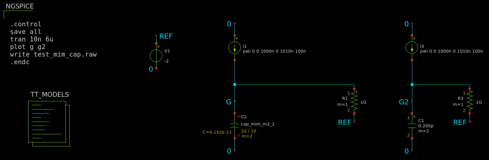
TEST MIM CAP
Metal-insulator-metal (MIM)

These capacitors are widely used because they exhibit high capacitance per unit area. To further enhance the capacitance value, MIM capacitors are typically constructed using three plates, two metal layers from the standard fabrication process (which often are the topmost layers), and a special metal layer in the middle. This unique arrangement allows MIM capacitors to achieve higher capacitance density while maintaining the advantages of stable performance and low leakage associated with their insulating dielectric material.
Advantages of metal-insulator-metal capacitors
Stable capacitance
High capacitance per unit area
Good quality factor
Good linearity
Disadvantages of metal-insulator-metal capacitors
Special process required to create masking layers
Increased cost
Schematic
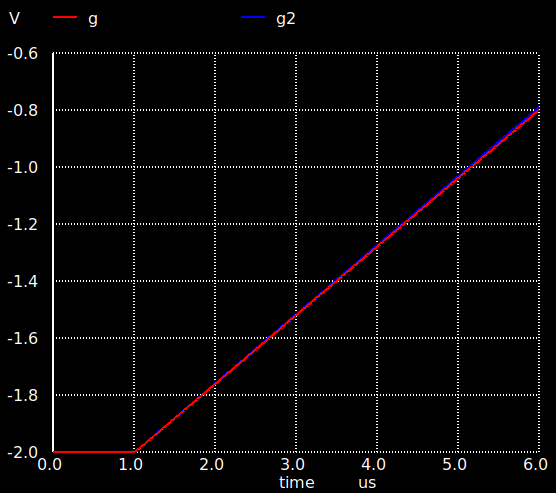
Simulation Results
Conclude
MIM Cap Layer: Need check later in layout
MIM Cap sizing: 10u*10u*2
MIM Capacitance: 0.41pF
TEST MOS CAP:
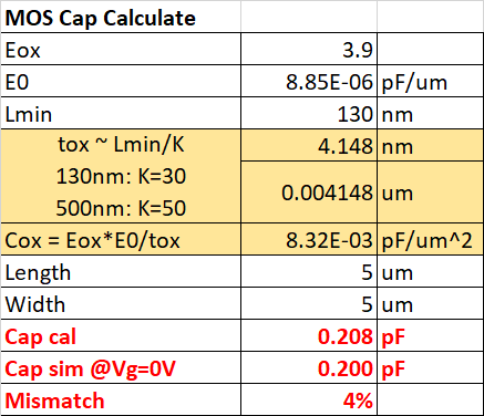
MOS Cap
Metal-oxide-semiconductor (MOS) capacitors are essentially a transistor that is used as a capacitor.
The capacitance value of MOS capacitors depends on the DC voltage applied at the gate. The varying voltage changes the depletion areas at the gate, altering the dielectric properties and subsequently modifying the capacitance. MOS capacitors are particularly useful for local supply decoupling applications, in which the DC voltage remains constant.
Advantages of metal-oxide-semiconductor capacitors
Exhibits higher capacitance per unit area compared to MIM capacitors
Has a thinner insulator (SiO2) at the gate
Disadvantages of metal-oxide-semiconductor capacitors
Significant variation in capacitance, with voltage limiting usage
Parasitic resistance from the bottom plate impacts performance
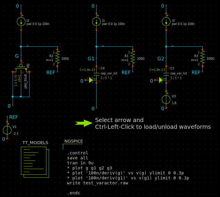
Schematic
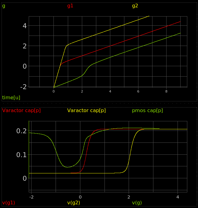
Simulation Results
Conclude
PMOS Sizing: 5u*5u*1
PMOS Cap: 0.2pF at 2V
Need to double check the Capacitance equation for MOS.
Confirmed: Eox*E0 = 0.34pF/cm can be used for calculate.
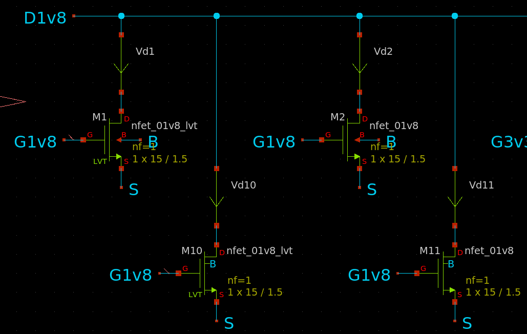
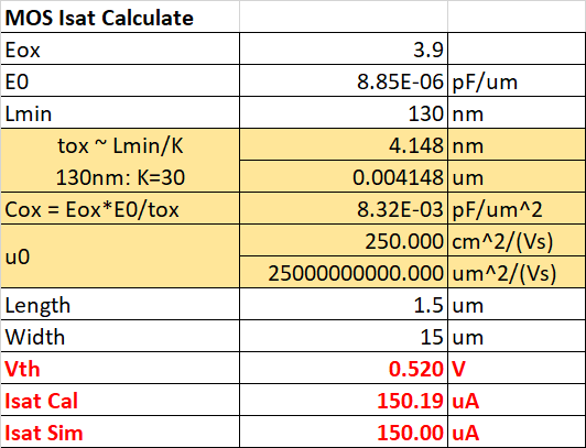
TEST NMOS
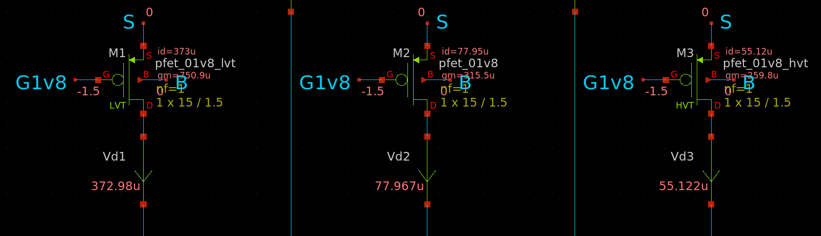
Schematic
Choose L=1.5u to ignore Channel Length Modulation Effect
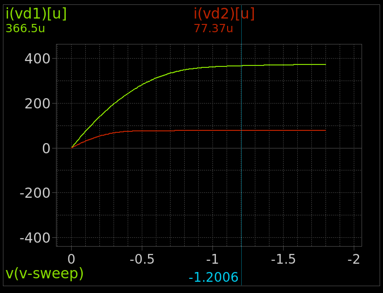
Simulation Results
VGS=0.9V
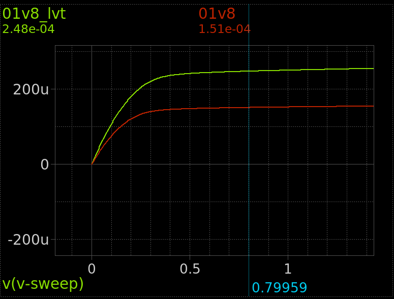
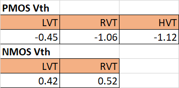
Conclude
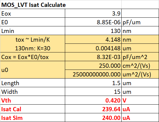
Apply u0=250 cm²/(Vs) for NMOS
TEST PMOS
Schematic
Simulation Result
Conclude
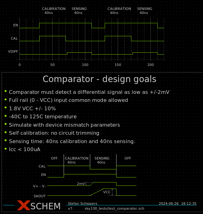
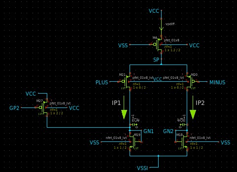
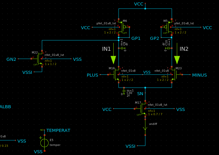
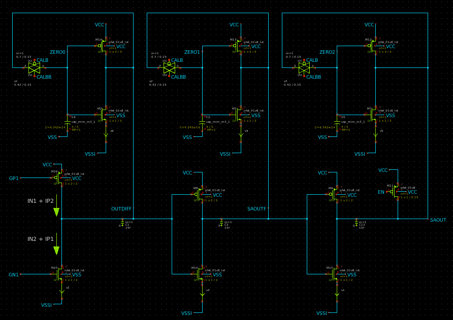
TEST COMPARATOR
Specification
Schematic
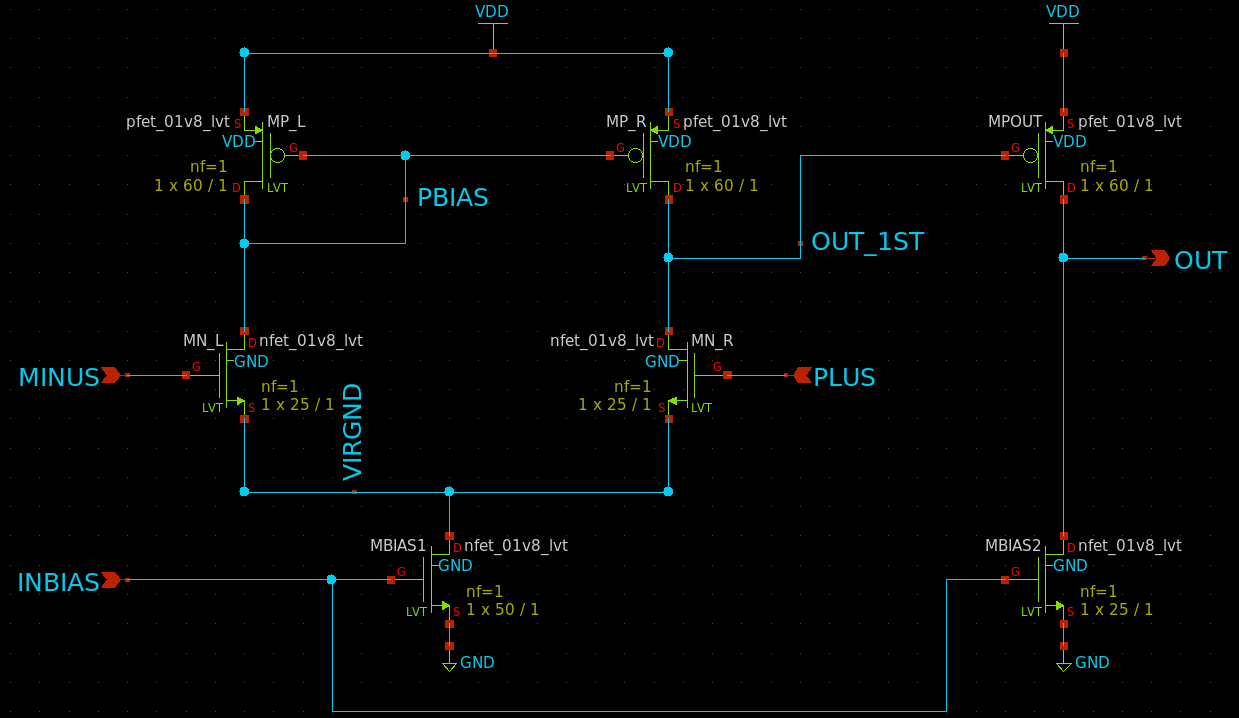
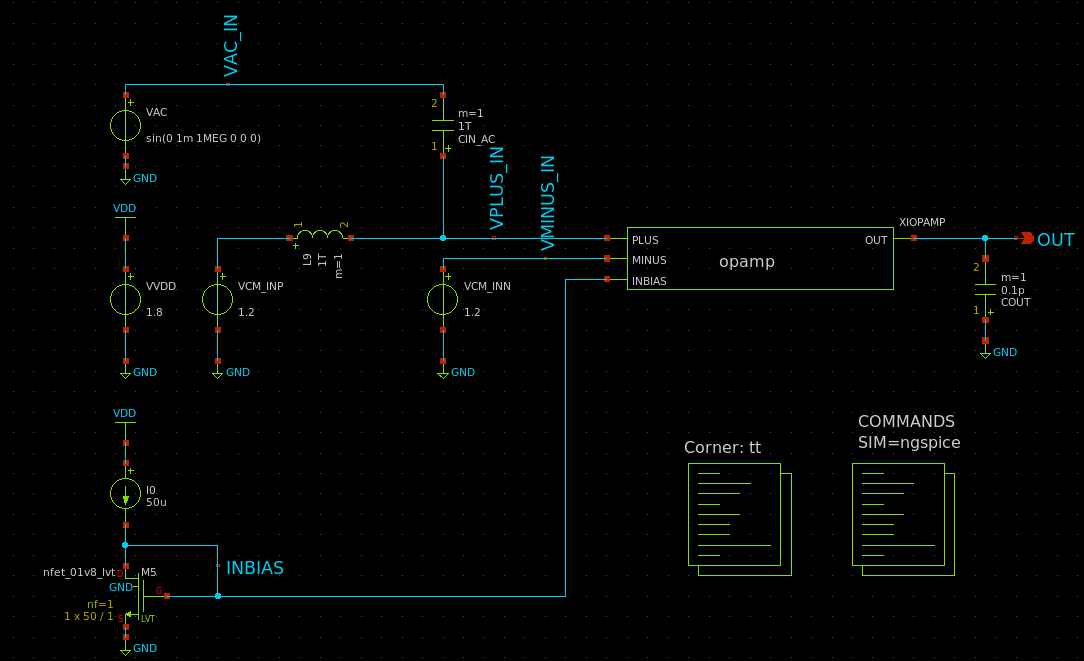
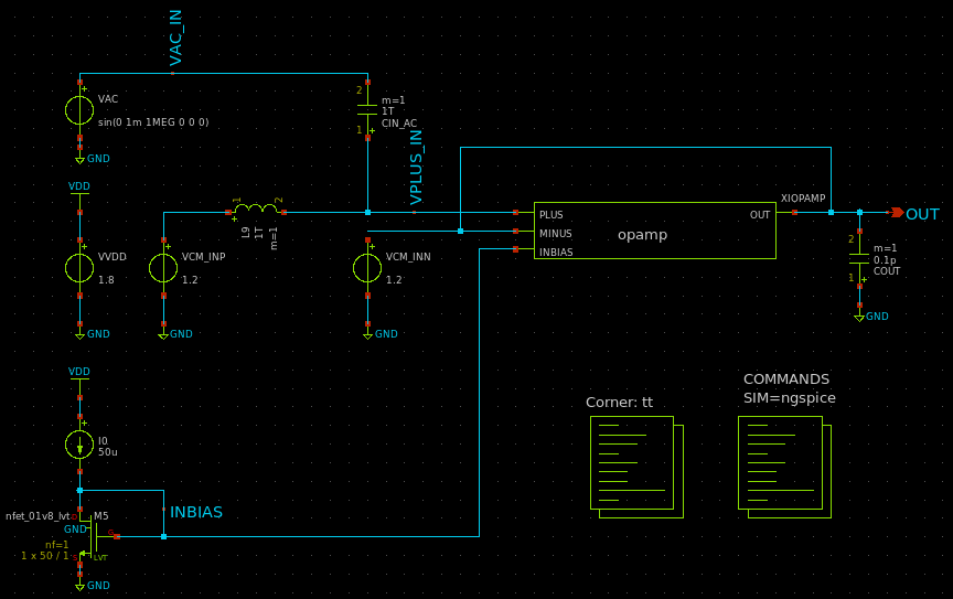
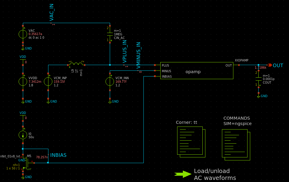
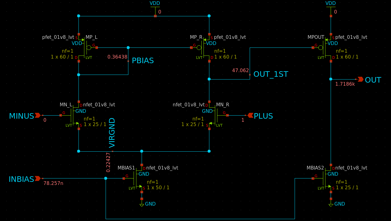
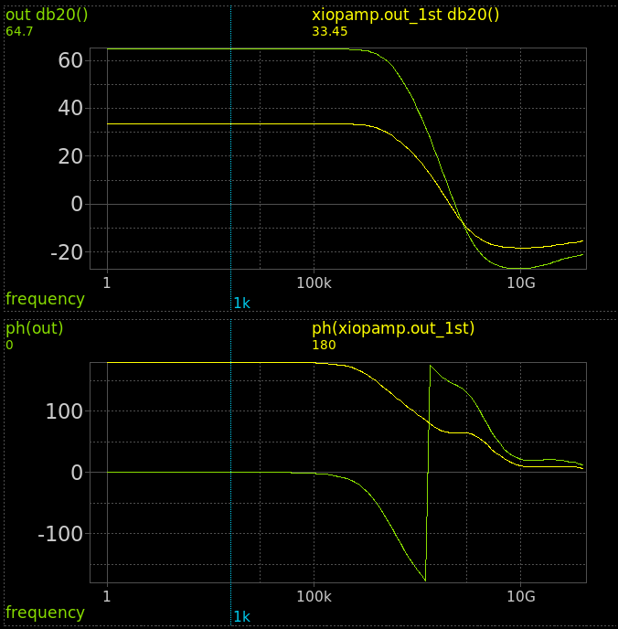
TWO STAGES OPAMP
Schematic
OP Analysis
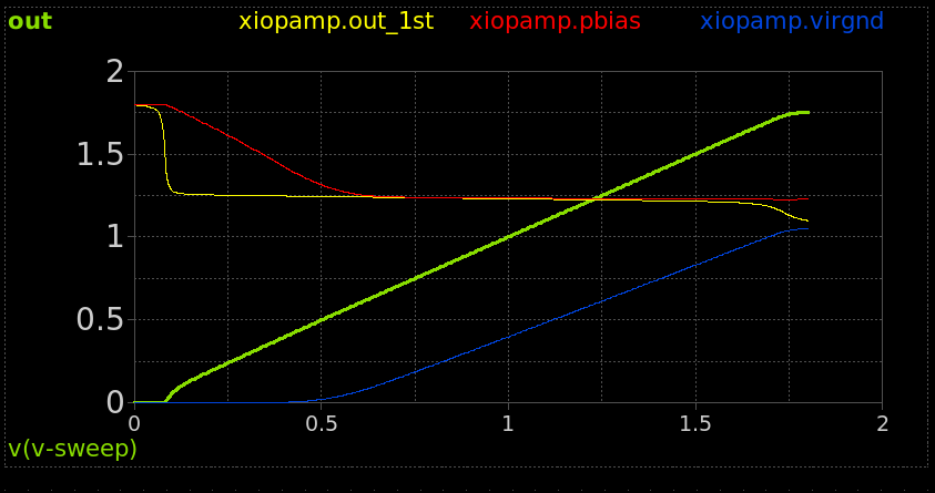
DC Analysis
Open loop:
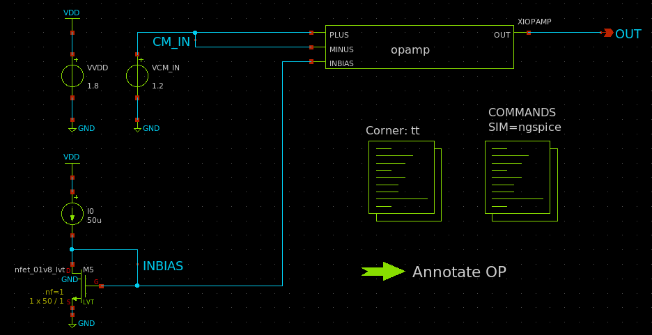
Close loop:
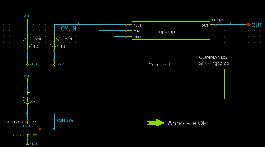
TRAN Analysis
Open loop:
Close loop:
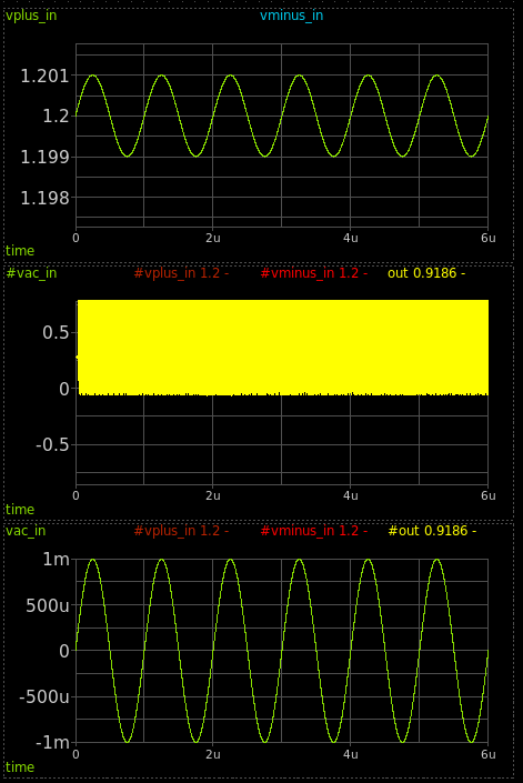
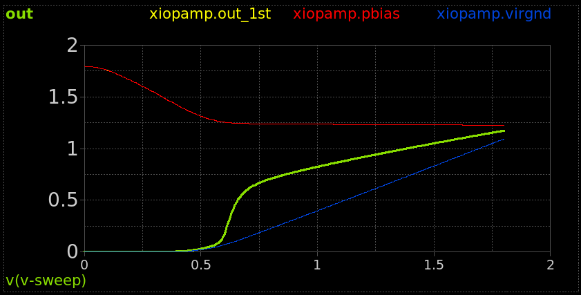
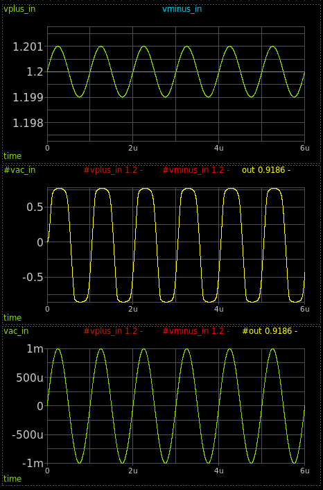
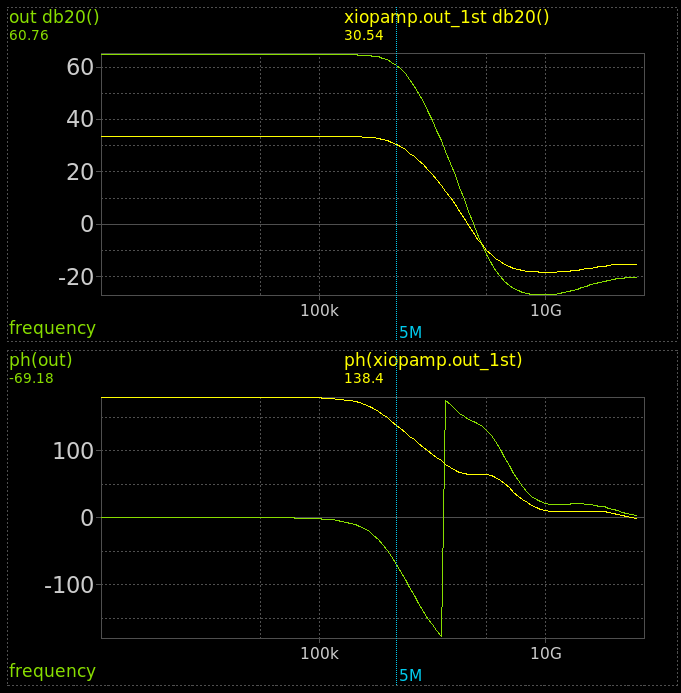
AC Analysis
Open loop:
Very small loading cap in OUT:
Close loop: