CMOS VLSI DESIGN
Chapter 1: Introduction
Chapter 2: MOS Transistor Theory
Chapter 3: CMOS Processing Technology
3.2 CMOS Technologies
CMOS processing steps can be broadly divided into two parts. Transistors are formed in the Front-End-of-Line (FEOL) phase, while wires are built in the Back-End-of-Line (BEOL) phase.
3.3 Layout Design Rules
The rules are defined in terms of feature sizes (widths), separations, and overlaps. The main objective of the layout rules is to build reliably functional circuits in as small an area as possible.
3.3.1 Design Rule Background
3.3.1.1 Well Rules
The n-well is usually a deeper implant (especially a deep n-well) than the transistor source/drain implants, and therefore, it is necessary to provide sufficient clearance between the n-well edges and the adjacent n+ diffusions.
Because the n-well sheet resistance can be several k< per square, it is necessary to ground the well thoroughly by providing a sufficient number of well taps. This will prevent excessive voltage drops due to well currents.
Where wells are connected to different potentials (say in analog circuits), the spacing rules may differ from equipotential wells (all wells at the same voltage––the normal case in digital logic).
3.3.1.2 Transistor Rules
CMOS transistors are generally defined by at least four physical masks.
active (also called diffusion, diff, thinox, OD, or RX)
n-select (also called n-implant, nimp, or nplus)
p-select (also called p-implant, pimp, or pplus)
polysilicon (also called poly, polyg, PO, or PC)
3.3.1.3 Contact Rules
There are several generally available contacts
Metal to p-active (p-diffusion)
Metal to n-active (n-diffusion)
Metal to polysilicon
Metal to well or substrate
3.3.1.4 Metal Rules
Metal rules may be complicated by varying spacing dependent on width: As the width increases, the spacing increases.
Metal overlap over contact might be zero or nonzero.
3.3.1.5 Via Rules
Vias are normally of uniform size within a layer. They may increase in size toward the top of a metal stack. For instance, large vias required on power busses are constructed from an array of uniformly sized vias.
3.3.1.6 Other Rules
Extension of polysilicon or metal beyond a contact or via
Differing gate poly extensions depending on the device length
Maximum width of a feature
Minimum area of a feature (small pieces of photoresist can peel off and float away)
Minimum notch sizes (small notches are rarely beneficial and can interfere with resolution enhancement techniques)
3.4 CMOS Process Enhancements
3.4.1 Transistors
3.4.1.1 Multiple Threshold Voltages and Oxide Thicknesses
Some processes offer multiple threshold voltages and/or oxide thicknesses.
Multiple masks and implantation steps are used to set the various thresholds.
3.4.1.3 High-k Gate Dielectrics
MOS transistors need high gate capacitance to attract charge to the channel. This leads to very thin SiO2 gate dielectrics. Gate leakage increases unacceptably below these thicknesses.
Gates could use thicker dielectrics and hence leak less if a material with a higher dielectric constant were available. (High-K Gate Dielectrics).
3.4.1.4 Higher Mobility
Increasing the mobility (R) of the semiconductor improves drive current and transistor speed. One way to improve the mobility is to introduce mechanical strain in the channel. This is called strained silicon.
3.4.1.5 Plastic Transistors
MOS transistors can be fabricated with organic chemicals. These transistors show promise in active matrix displays, flexible electronic paper, and radio-frequency ID tags because the devices can be manufactured from an inexpensive chemical solution.
3.4.1.6 High-Voltage Transistors
High-voltage MOSFETs can also be integrated onto conventional CMOS processes for switching and high-power applications. Gate oxide thickness and channel length have to be larger than usual to prevent breakdown.
3.6 Manufacturing Issues
3.6.1 Antenna Rules
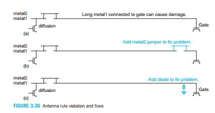
When a metal wire contacted to a transistor gate is plasma-etched, it can charge up to a voltage sufficient to zap the thin gate oxides. This is called plasma-induced gate-oxide damage, or simply the antenna effect.
It can increase the gate leakage, change the threshold voltage, and reduce the life expectancy of a transistor. Longer wires accumulate more charge and are more likely to damage the gates.
Antenna rules specify the maximum area of metal that can be connected to a gate without a source or drain to act as a discharge element. Larger gates can withstand more charge buildup. The design rules normally define the maximum ratio of metal area to gate area such that charge on the metal will not damage the gate. The ratios can vary from 100:1 to 5000:1 depending on the thickness of the gate oxide (and hence breakdown voltage) of the transistor in question.