EE 2501 Digital Logic Design Homework Notes
Page 1: Creating the State Table and Logic Diagram
State Table Structure
Present State: Defines the current state of the system.
Input: Represents inputs X, QA, QB that influence state transitions.
Next State: Outcomes based on current states and inputs. Indicates where the system will transition based on input and present state.
Output: Indicates what output (Y) results from state and input combinations. Outputs are derived from the logical combination of present states and inputs.
Example State Table
Present State (QA, QB) | Input X | Next State | Output Y |
|---|---|---|---|
(0, 0) | 0 | (0, 0) | 0 |
(0, 0) | 1 | (0, 1) | 0 |
(0, 1) | 0 | (1, 1) | 1 |
(0, 1) | 1 | (1, 0) | 0 |
(1, 0) | 0 | (0, 0) | 0 |
(1, 0) | 1 | (1, 1) | 1 |
(1, 1) | 0 | (1, 0) | 0 |
(1, 1) | 1 | (0, 0) | 0 |
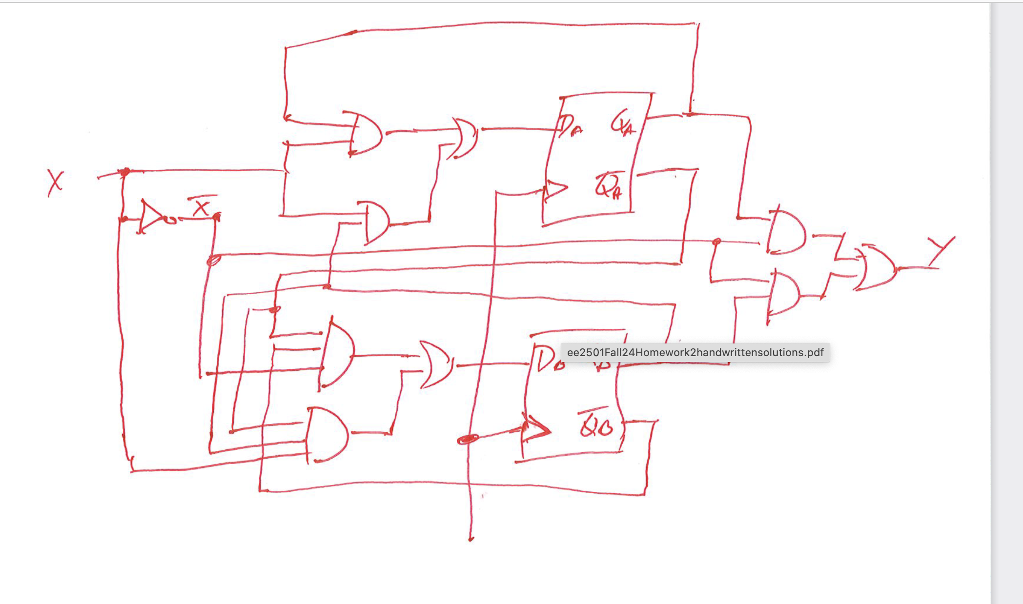
Logic Diagram
Utilize the transitions from the state table to create the logic diagram, showing how the outputs depend on inputs. A logic diagram visually represents the relationships of inputs and outputs, often using gates such as AND, OR, and NOT.
Page 2: State Table Assuming All Flip-Flops are Zero
Flip-Flop Model
The model assumes initial states Q1, Q2, Q4, Q8 are all zero.
Inputs: C1, J1, K1, and their counterparts for the second flip-flop.
Example of State Transitions
Current State | Input Conditions | Next State |
|---|---|---|
0 | J=1, K=0 | 1 |
1 | J=0, K=1 | 0 |
0 | J=1, K=1 | Toggle |
Transition Analysis
Analyzing how each bit transitions based on the input conditions and standalone characteristics of J-K flip-flops, which toggle on certain combinations of J and K inputs. A J-K flip-flop is a type of digital storage element, where the next state depends on the J (set) and K (reset) inputs.
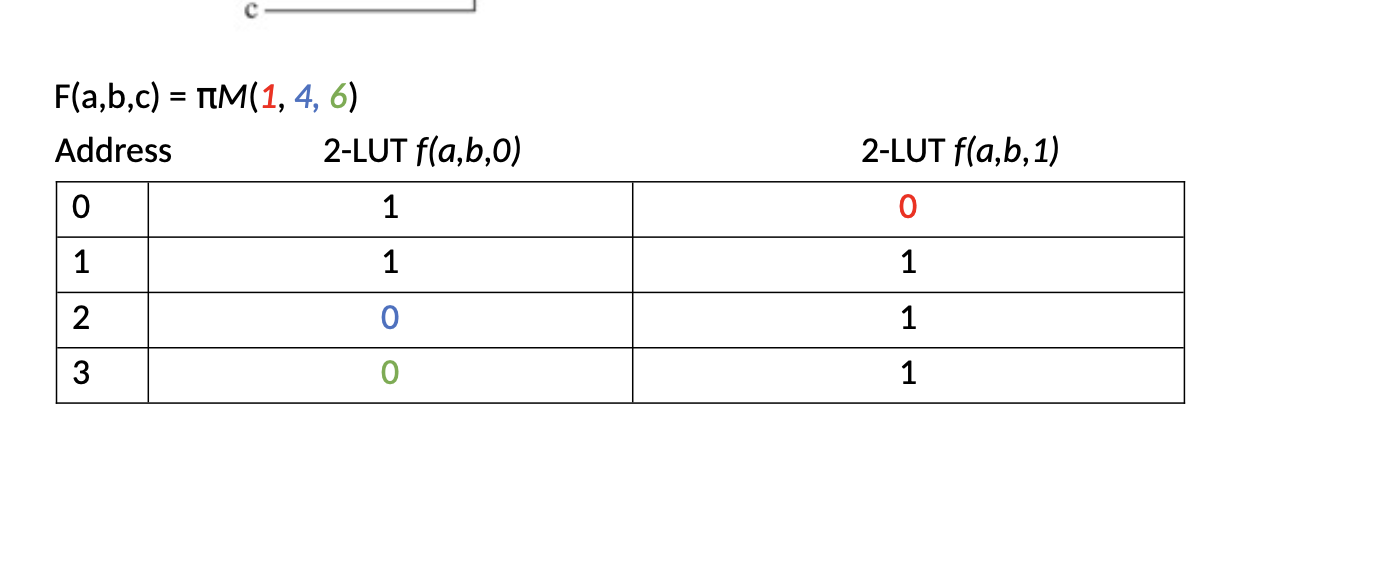
Page 3: Values for LUTs
Logic Implementation
Function: F(a,b,c) = πM(X, Y, Z) where:
X: lowest non-zero digit from KSU ID.
Z: highest digit ≤ 7 from KSU ID.
Y: any digit between
XandZ.
Example Calculation
Example LUT addresses:
Control Inputs: Di, S1, S0 dictate the operation of the register (Data Input, Shift Left/Right).
Operation: load data, shift left or right.
Calculation Example
If Di = 1, S1 = 1, S0 = 1:
Next State Value: Qi = Di since load operation is performed.
Operation: Load, which means taking the input data into the register.
Page 5: D-Latch and D-FlipFlop Output Waveform
D-Latch Waveform Sketch
Initial Q: 0 before clock triggers.
Clock Phase: When clock is high, follow the data signal to update output Q. A D-latch is a storage device that captures input data when the clock is high.
D-FlipFlop Waveform Sketch
Similar principles apply:
Clock Sensitivity: Q updates only on rising edge of the clock signal, ensuring synchronous operation.
Consider Propagation Delays: Assume negligible for clarity in design, but note that actual designs must account for these delays.
Conclusion
Understanding state tables, logic diagrams, LUTs, shift registers, and latch/flip-flop mechanisms is fundamental in digital logic design.
Definitions
Karnaugh Mapping (K-mapping): A method for simplifying Boolean algebra expressions that provides a visual representation of truth tables. It allows for systematic grouping of terms to minimize the number of logical operations needed.
Boolean Algebra: A mathematical structure that captures the essence of logical reasoning, used in logic circuit design and simplification. It consists of binary variables and operations such as AND, OR, and NOT, forming the basis for designing logical circuits and for simplifying logic expressions efficiently.
Clock Sensitivity: Refers to the characteristic of certain digital circuits, particularly flip-flops, whereby the output state changes only in response to the edges (either rising or falling) of a clock signal. In synchronous systems, clock sensitivity ensures that the flip-flop will sample its input and potentially change its output only at these designated moments. This control mechanism is vital for maintaining reliable and predictable operation of sequential circuits, allowing for stable data capture during specific time intervals dictated by the clock.
Timing of Gate Usage
AND Gate: Use when you need the output to be true only when all input conditions are met. For example, in a scenario where two inputs represent two sensors, and you want the output to activate a system only if both sensors are triggered (logic 1).
OR Gate: Utilize when the output should be true if at least one input condition is satisfied. For instance, if an alarm should sound when either of two security sensors is triggered, then an OR gate will combine the inputs.
Diagram Construction Steps:
Start by identifying all inputs and outputs based on the state table.
For each output in the state table, analyze the conditions under which it is true based on the inputs and present states.
Implement logical relationships using the appropriate gates as determined in the previous steps.
Connect inputs to their corresponding logic gates, ensuring you correctly reflect the conditions that lead to each output.
Review the completed logic diagram to ensure that all cases from the state table are accurately represented, refining as necessary to maintain clarity and correctness.
Logic Diagram Creation
Identify when to use an AND gate: Implement in scenarios where all inputs must be true for the output to be true, such as turning on a system only when multiple safety sensors are activated.
Determine when to use an OR gate: Utilize for circumstances where at least one input must be true—for example, setting off an alarm when any one of several security sensors is triggered.
Construct the logic diagram by drawing gates and connecting them per the output sections from the state table.
Ensure clarity by labeling all inputs, outputs, and components accurately in the diagram for ease of understanding and implementation.
Flip-Flop Transition Analysis
Model transitions of each flip-flop (Q1, Q2, Q4, Q8) with defined initial conditions (usually all zeros).
Analyze the relationship between J and K inputs for the J-K flip-flop, noting toggle conditions for state transitions.
Document the transition rules based on various input conditions (for instance, J=1, K=0 leads to setting the flip-flop to 1).
LUT Values Implementation
Define a logic function F(a,b,c) = πM(X, Y, Z) where X is the lowest non-zero digit from an identifier like a student ID.
Calculate specific LUT values by determining the required maxterms based on the ID.
Create an address-value table that maps each address to its corresponding value according to the logic function results.
Ensure that this table includes all possible conditions and corresponds accurately to the function defined.
Shift Operation Control Steps to Solve Bidirectional Shift Register Problem:
Identify the control inputs:
From the problem: S1 = 1, S0 = 1
Determine which MUX input is selected:
Use the control inputs as a binary index
→s1s0=11 selects MUX input 3
Find what is connected to MUX input 3:
According to the diagram, input 3 is Dᵢ
Understand what the MUX output feeds:
MUX output goes to the D input of flip-flop Qᵢ
Evaluate what happens on the next positive clock edge:
Flip-flop Qᵢ will load the value of Dᵢ
Determine the operation performed:
Since data is loaded directly from Dᵢ, this is a Load operation
Answer the question:
Which value will Qᵢ take? → Dᵢ
Operation being performed? → Load
D-Latch and D-FlipFlop Waveform Analysis
Change Q only when C is HIGH
Copy D during C=1
Hold Q value when C=0
D-Latch should:
Change Q only when C is HIGH
Copy D during C=1
Hold Q value when C=0
An idea of what the ogic digram for a state table is supposed to look like