Bandgap References Notes
Bandgap References
Analog circuits rely heavily on voltage and current references, which are DC quantities with minimal dependence on supply and process parameters, and a defined temperature dependence.
These references are crucial for:
Biasing differential pairs to ensure stable voltage gain and noise.
Defining common-mode levels in operational amplifiers (op-amps).
Establishing full-scale ranges in A/D and D/A converters.
12.1 General Considerations
The goal of reference generation is to create a stable DC voltage or current that is independent of supply and process variations and exhibits a well-defined behavior with temperature.
Temperature dependence can take three forms:
Proportional to absolute temperature (PTAT).
Constant-Gm behavior, where the transconductance of transistors remains constant.
Temperature independence.
Design considerations include:
Supply-independent biasing.
Defining temperature variation.
Output impedance.
Output noise.
Power dissipation.
12.2 Supply-Independent Biasing
Ideal bias currents and current mirrors assume the availability of a stable reference current I{REF}. If I{REF} is independent of V{DD}, and channel-length modulation is negligible, then I{D2} and I{D3} remain independent of the supply voltage. However, generating I{REF} presents a challenge.
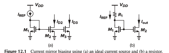
Using a resistor tied to V{DD} as a current source approximation is sensitive to V{DD}.
\frac{\Delta I{out}}{\Delta V{DD}} = \frac{1}{R1 + 1/g{m1}} \frac{(W/L)2}{(W/L)1}
Bootstrapping can create a self-biasing circuit where I{REF} is derived from I{out}, making it independent of V{DD}. In this configuration, I{out} = KI_{REF}.
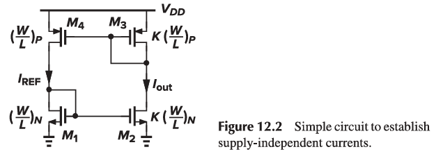
Since I{out} and I{REF} are relatively independent of V{DD}, their magnitude is determined by other parameters. If transistors M1-M4 operate in saturation and \lambda \approx 0, then I{out} = KI_{REF}, meaning the circuit can support any current level. To uniquely define the currents, an additional constraint must be added to the circuit.
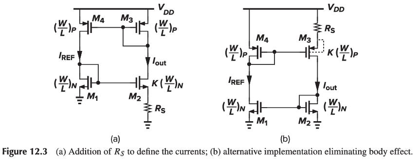
Adding a resistor RS decreases the current of M2. The PMOS devices ensure that I{out} = I_{REF}. We can express this mathematically as:
V{GS1} = V{GS2} + I{D2}RS
2\sqrt{\frac{I{out}}{\mun C{ox} (W/L)N}} + V{TH1} = 2\sqrt{\frac{I{out}}{\mun C{ox} K(W/L)N}} + V{TH2} + I{out}RS
I{out} = \frac{2}{\mun C{ox} (W/L)N R_S^2} (1-\frac{1}{\sqrt{K}})^2
Placing the resistor in the source of M3 eliminates the body effect and maintains supply independence if channel-length modulation is negligible.
Long channels are used to further minimize channel-length modulation and reduce flicker noise.
The “gain” from V{DD} to I{out} can be calculated using small-signal analysis. The sensitivity vanishes if r_{04} = \infty.
G{m2} = \frac{g{m2}r{02}}{RS r{02}(g{m2} + g{mb2}) + RS r_{02}}
An important issue in supply-independent biasing is the existence of degenerate bias points. For example, in the circuit of Fig. 12.3(a), if all transistors carry zero current when the supply is turned on, they may remain off indefinitely because the loop can support a zero current in both branches. This condition is not predicted by (12.4) because in manipulating (12.3), we divided both sides by I{out}, tacitly assuming that I{out} \neq 0. In other words, the circuit can settle in one of two different operating conditions.
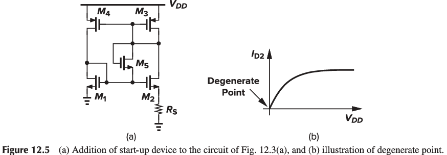
Also called the “start-up” problem, the above issue is resolved by adding a mechanism that drives the circuit out of the degenerate bias point when the supply is turned on. M5 provides a current path from V_{DD} through M3 and M1 to ground upon start-up, thereby preventing them from remaining off.
12.3 Temperature-Independent References
Temperature-independent reference voltages or currents are crucial because most process parameters vary with temperature. A temperature-independent reference is usually process-independent as well.
By adding two quantities with opposite temperature coefficients (TCs) with proper weighting, the result displays a zero TC. For two voltages V1 and V2 with opposite TCs, choose \alpha1 and \alpha2 such that \alpha1 V1/T + \alpha2 V2/T = 0, obtaining a reference voltage, V{REF} = \alpha1 V1 + \alpha2 V_2, with zero TC.
12.3.1 Negative-TC Voltage
The base-emitter voltage of bipolar transistors or the forward voltage of a pn-junction diode exhibits a negative TC.
For a bipolar device, IC = IS exp(V{BE}/VT), where VT = kT/q. The saturation current IS is proportional to \mu k T ni^2, where \mu is the mobility of minority carriers and ni is the intrinsic carrier concentration of silicon. The temperature dependence of these quantities is represented as \mu \propto T^m, where m \approx -3/2, and ni^2 \propto T^3 exp[-Eg/(kT)], where E_g \approx 1.12 eV is the bandgap energy of silicon.
IS = bT^{4+m}exp(-\frac{Eg}{kT})
Writing V{BE} = VT ln(IC/IS), the TC of the base-emitter voltage can be computed:
\frac{\partial V{BE}}{\partial T} = \frac{\partial VT}{\partial T} ln(\frac{IC}{IS}) - VT \frac{\partial IS}{\partial T}
For constant I_C:
\frac{VT}{IS} \frac{\partial IS}{\partial T} = (4+m) \frac{VT}{T} + \frac{Eg}{kT^2} VT
\frac{\partial V{BE}}{\partial T} = \frac{VT}{T} ln(\frac{IC}{IS}) - (4+m)\frac{VT}{T} - \frac{Eg/q}{kT^2/T} V_T
\frac{\partial V{BE}}{\partial T} = \frac{V{BE} - (4+m) VT - Eg/q}{T}
12.3.2 Positive-TC Voltage
If two bipolar transistors operate at unequal current densities, the difference between their base-emitter voltages is directly proportional to the absolute temperature.
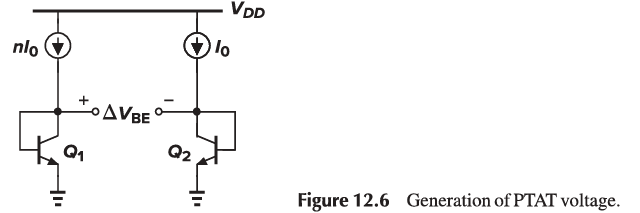
If two identical transistors (I{S1} = I{S2}) are biased at collector currents of nIO and IO:
\Delta V{BE} = V{BE1} - V{BE2} = VT ln(\frac{nIO}{I{S1}}) - VT ln(\frac{IO}{I{S2}}) = VT ln(n)
\frac{\partial \Delta V_{BE}}{\partial T} = \frac{k}{q} ln(n)
If Q2 is formed as the parallel combination of m units, each identical to Q1:
\Delta V{BE} = VT ln(\frac{nIO}{IS}) - VT ln(\frac{IO}{mIS}) = VT ln(nm)
12.3.3 Bandgap Reference
A reference with a nominally zero temperature coefficient can be developed using negative- and positive-TC voltages.
V{REF} = \alpha1 V{BE} + \alpha2(VT ln(n)), where VT ln(n) is the difference between the base-emitter voltages of two bipolar transistors operating at different current densities.
At room temperature, \frac{\partial V{BE}}{\partial T} \approx -1.5 mV/K whereas \frac{VT}{T} \approx +0.087 mV/K. Set \alpha1 = 1 and choose \alpha2 ln(n) such that (\alpha2 ln(n)) (0.087 mV/K) = 1.5 mV/K. That is, \alpha2 ln(n) \approx 17.2, indicating that for zero TC:
V{REF} = V{BE} + 17.2 V_T \approx 1.25 V
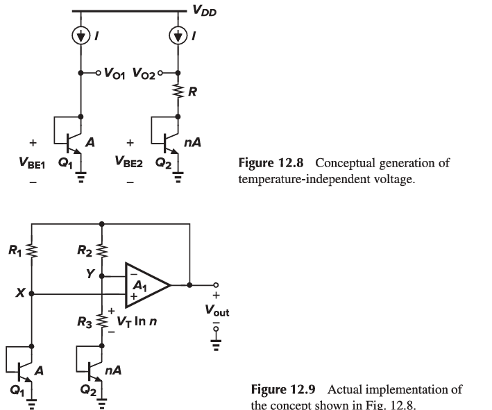
To make the circuit practical, a mechanism must be added to guarantee that V{O1} = V{O2}. Since ln(n) = 17.2 translates to a prohibitively large n, the term RI = VT ln(n) must be scaled up by a reasonable factor. Then, V{O2}, which is somehow forced to be equal to V{O1}, cannot become temperature-independent because V{O2} \approx V{BE1} \approx 800 mV, whereas, for temperature independence, we must have V{O2} = V{BE2} + 17.2 VT \approx 1.25 V.
V{out} = V{BE2} + \frac{VT ln(n)}{R3}(R3 + R2) = V{BE2} + (VT ln(n))(1 + \frac{R2}{R3})
For a zero TC, we must have (1 + R2/R3) ln(n) \approx 17.2.
Collector Current Variation
In the circuit of Fig. 12.9, the collector currents of Q1 and Q2, given by (VT ln(n))/R3, are proportional to T, whereas \frac{\partial V_{BE}}{\partial T} \approx -1.5 mV/K was derived for a constant current.
Returning to Eq. (12.9) and including \frac{\partial I_C}{\partial T}, we have:
\frac{\partial V{BE}}{\partial T} = \frac{\partial VT}{\partial T} ln(\frac{IC}{IS}) + VT (\frac{1}{IC} \frac{\partial IC}{\partial T} - \frac{1}{IS} \frac{\partial I_S}{\partial T})
Since \frac{IC}{\partial T} \approx (VT ln(n))/(R3 T) = \frac{IC}{T}, we can write:
Equation (12.13) is therefore modified as:
\frac{\partial V{BE}}{\partial T} = \frac{V{BE} - (3+m) VT - Eg/q}{T}
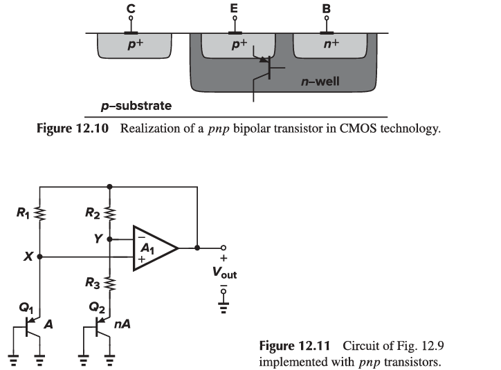
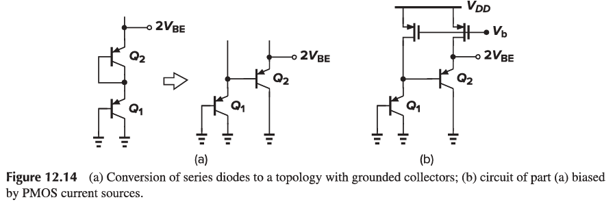
Compatibility with CMOS Technology
In n-well processes, a pnp transistor can be formed using a p+ region inside an n-well as the emitter and the n-well itself as the base. The p-type substrate acts as the collector. The circuit of Fig. 12.9 can therefore be redrawn as shown in Fig. 12.11.
Op Amp Offset and Output Impedance
The input offset voltage of the op amp in Fig. 12.9 introduces error in the output voltage. The effect is quantified as:
V{out} = V{BE2} + \frac{R3 + R2}{R3} (VT ln(n) - V_{OS})
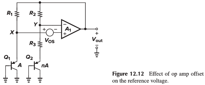
The key point here is that Vos is amplified by 1 + R2/R3, introducing error in V_{out}. More importantly, Vos itself varies with temperature, raising the temperature coefficient of the output voltage.
The small-signal gain from V{OS} to V{out} in Fig. 12.12 is:
\frac{V{out}}{V{OS}} = -\frac{1 + gm R2}{(1/gm + R2) + \frac{R2}{R3}}
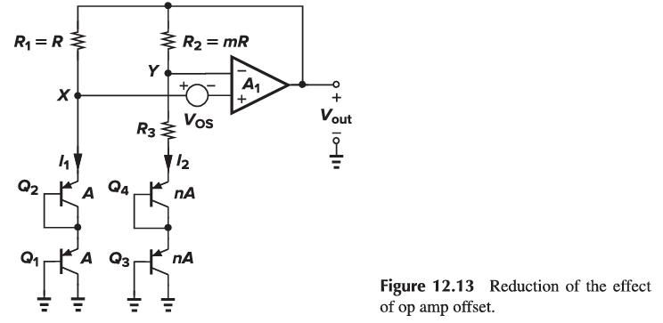
Several methods are employed to lower the effect of Vos.
The op amp incorporates large devices in a carefully chosen topology so as to minimize the offset (Chapter 19).
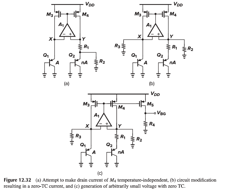
The collector currents of Q1 and Q2 can be ratioed by a factor of m such that \Delta V{BE} = VT ln(mn).
Each branch may use two pn junctions in series to double \Delta V_{BE}.
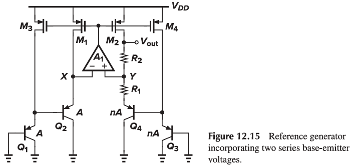
The implementation of Fig. 12.13 is not feasible in a standard CMOS technology because the collectors of Q2 and Q4 are not grounded.
Feedback Polarity
In the circuit of Fig. 12.9, the feedback signal produced by the op amp returns to both of its inputs. The negative-feedback factor is given by:
\betaN = \frac{1/g{m2} + R3}{1/g{m2} + R3 + R2}
and the positive-feedback factor by:
\betaP = \frac{1/g{m1}}{1/g{m1} + R1}
To ensure an overall negative feedback, \betaP must be less than \betaN, preferably by roughly a factor of two so that the circuit’s transient response remains well behaved with large capacitive loads.
The voltage generated according to (12.20) is called a “bandgap reference.” The term “bandgap” is used here because as T \rightarrow 0, V{REF} \rightarrow Eg/q.
We can write the output voltage as:
V{REF} = V{BE} + V_T ln(n)
Taking the derivative with respect to temperature:
\frac{\partial V{REF}}{\partial T} = \frac{\partial V{BE}}{\partial T} + ln(n) \frac{\partial V_{T}}{\partial T}
Setting this to zero and substituting for \frac{\partial V_{BE}}{\partial T} from (12.13), we have:
V{REF} = \frac{Eg}{q} + (4+m) V_T
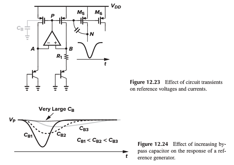
Supply Dependence and Start-Up
The circuit may require a start-up mechanism because if Vx and Vy are equal to zero, the input differential pair of the op amp may turn off. Start-up techniques similar to those of Fig. 12.5 can be added to ensure that the op amp turns on when the supply is applied.
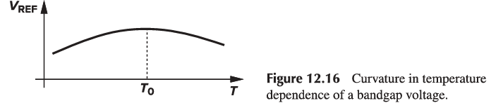
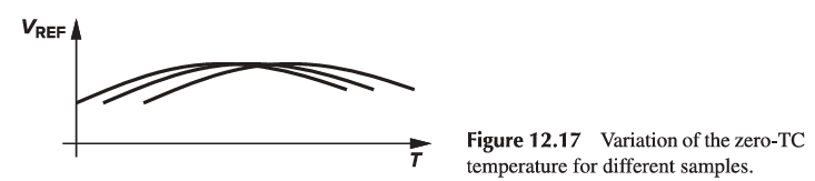
Curvature Correction
If plotted as a function of temperature, bandgap voltages exhibit a finite “curvature,” i.e., their TC is typically zero at one temperature and positive or negative at other temperatures.
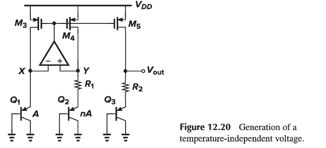
12.4 PTAT Current Generation
PTAT currents can be generated by a topology such as that shown in Fig. 12.18. For low-voltage operation, the topology of Fig. 12.18 is preferred.
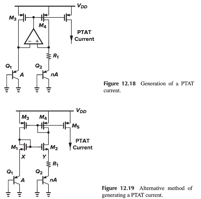
The circuit of Fig. 12.18 can be readily modified to provide a bandgap reference voltage as well. The output therefore equals
V{REF} = V{BE3} + \frac{R2}{R1} V_T ln(n)
12.5 Constant-Gm Biasing
The transconductance of MOSFETs plays a critical role in analog circuits, determining such performance parameters as noise, small-signal gain, and speed.
A simple circuit to define the transconductance is the supply-independent bias topology of Fig. 12.3. The bias current is given by:
I{out} = \frac{2}{\mun C{ox} (W/L)N R_S^2}(1-\frac{1}{\sqrt{K}})^2
Thus, the transconductance of M1 equals
g{m1} = 2 \sqrt{\mun C{ox} (\frac{W}{L})N I{D1}} = \frac{1}{RS} (1-\frac{1}{\sqrt{K}})
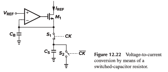
A Switched-Capacitor “Resistor” can also be implemented.
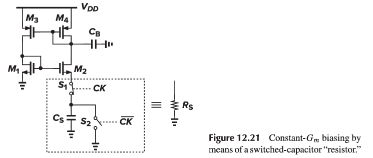
The switched-capacitor approach of Fig. 12.21 can be applied to other circuits as well. For example, a voltage-to-current converter with a relatively high accuracy can be constructed.
12.6 Speed and Noise Issues
The output noise of reference generators may affect the performance of low-noise circuits considerably. Figure 12.28 illustrates an example: the load current source of a common-source stage is driven by a bandgap circuit with a current multiplication factor of N. Thus, the noise current of M1 (or M2) is amplified by the same factor as it appears in M3.
As another example, if a high-precision A/D converter employs a bandgap voltage as the reference with which the analog input signal is compared , then the noise in the reference is directly added to the input.
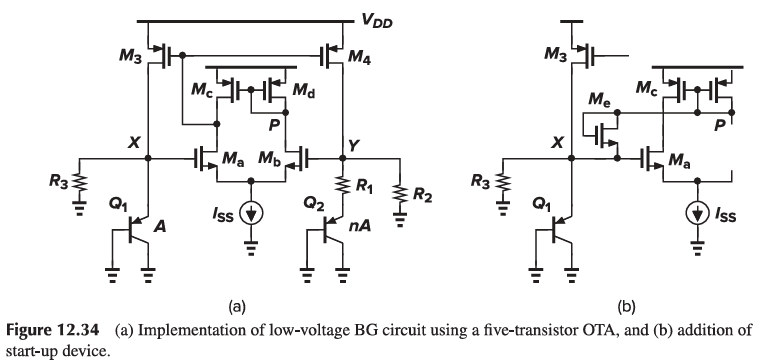
12.7 Low-Voltage Bandgap References
The fundamental limitation is that about 17.2VT must be added to one VBE so as to achieve a net zero temperature coefficient.
Using the topology of Fig. 12.32 lends itself to low-voltage implementation, requiring a minimum VDD of V{be1} + |V{ds3}|.
To analyze the circuit, we observe that Vx ≈ Vy ≈ |V{BE1}| and I{D3} = I_{D4}. Thus,
I{C1} + \frac{|V{BE1}|}{R3} = I{C2} + \frac{|V{BE1}|}{R2}
which yields I{C1} = I{C2} if R2 = R3. We still have |V{BE1}| = |V{BE2}| + I{C2} R1 and hence I{C2} = VT ln \frac{n}{R1}. This current and the current flowing through R2, |V{BE1}|/R2, constitute |I_{D4}|:
|I{D4}| = \frac{VT ln n}{R1} + \frac{|V{BE1}|}{R2} = \frac{1}{R1} (|V{BE1}| + \frac{R2}{R1} VT ln n)
Selecting (\frac{R2}{R1}) VT ln n approximately equal to 17.2V renders a zero TC for I{D4}. This current is then copied and passed through a resistor to generate a zero-TC voltage
V{BG} = \frac{R4}{R2} (|V{BE1}| + \frac{R2}{R1} V_T ln n)
We choose (\frac{R2}{R1}) ln n ≈ 17.2, observing that VBG has a zero TC and its value can be lower than the conventional limit of 1.25 V.
Op amp input offset, Vos, produces:
V{BG} = \frac{R4}{R2} (|V{BE1}| + \frac{R2}{R1} VT ln n) - (1 + \frac{R2}{R1}) V{OS}
12.8 Case Study
M11 sets the gate voltage of M9 at V{BE4} + V{GS11}, establishing a voltage equal to V{BE4} across R6 if M9 and M11 are identical. Thus, I{D9} = \frac{V{BE4}}{R6}, yielding V{R4} = V{BE4} (\frac{R4}{R6}). Also, if M10 is identical to M2, then |I{D10}| = \frac{2 (VT ln n)}{R1}, and hence V{R5} = \frac{2(VT ln n) R5}{R_1}. Since the op amp ensures that VE ≈ VF, we have
V{out} = \frac{R4}{R6} V{BE4} + \frac{2 VT ln n R5}{R_1}