Computer Architecture, Systems Organisation, and Processor Instruction Sets
Fundamentals of Computer Architecture and Organisation
Definitions and Distinction:
Computer Architecture refers to the architectural attributes of a system that directly impact the logical execution of a program.
Computer Organisation refers to the operational units and their physical interconnections that realize an architectural specification, directly affecting system price and performance.
Architectural Attributes:
The CPU instruction set.
The number of bits used to represent various data types (e.g., numbers, characters).
Input/Output (I/O) mechanisms.
Memory addressing techniques.
Organisational Attributes:
Hardware control signals.
Interfaces between the computer system and peripheral devices.
The specific memory technology utilized (e.g., SRAM, DRAM, flash memory).
Design Trade-off Example:
Architectural Design Issue: Deciding whether a computer system will feature a dedicated multiply instruction.
Organisational Design Issue: Deciding whether the multiply instruction is executed by a dedicated hardware multiply unit or through repeated calls to the arithmetic add unit (e.g., calculating vs. ).
Both implementations produce the exact same logical result. The design decision depends on the frequency of multiply instruction usage, the execution speed of both approaches, and the physical size and monetary cost of adding a dedicated multiply unit.
Computer Families:
Manufacturers frequently offer a family of computer models. All models within a family share an identical computer architecture (ensuring software compatibility) but possess different computer organisation, resulting in varying price and performance points.
Hardware Classification and Hierarchical System Structure
System Diversity:
Computers vary widely based on cost, performance, physical size, and target applications.
Commercial Brands: HP, Apple, Dell, Asus, Toshiba, Lenovo.
Computer Classifications: Desktop, Laptop, Tablet, Smart phone, Server, Supercomputer, Embedded Systems (e.g., Raspberry Pi), and Wearables.
Hierarchical System Structure:
Computers are inherently complex systems.
Understanding complex systems requires analyzing their hierarchical nature, breaking down interrelated subsystems, and drilling down to elementary physical and logical subsystems.
Component Relationship:
Structure: The specific manner in which system components relate to one another.
Function: The operation of each individual component as part of the overarching structure.
Computer Functions and Functional Component Views
Four Fundamental Computer Functions:
Data Processing: Operations performed on data.
Data Storage: Short-term or long-term retention of data.
Data Movement: Transferring data between the computer and external devices or networks.
System Control: Managing processing, storage, and movement operations.
Operational Views of Data Flow:
Data Movement: Directly between the computer and external environments via peripherals (I/O devices) or over longer distances via data communication channels.
Storage Operations: Storing data temporarily (e.g., RAM) or permanently (e.g., files), executed via Read and Write functions.
Processing Operations: Performed directly on locally stored data or dynamically on data moving en route between local storage and external I/O environments.

Principal Elements of a Computer System:
Central Processing Unit (CPU / Processor): Controls overall system operations and performs data processing functions.
Main Memory: Stores active data and program instructions.
Input/Output (I/O) Subsystem: Transfers data between the computer and its external environment.
System Interconnection: The structural mechanism providing communication pathways among the CPU, main memory, and I/O subsystems.

Structural Subsystems of the CPU:
Control Unit (CU): Controls and coordinates all operations of the CPU.
Arithmetic and Logic Unit (ALU): Performs data processing, arithmetic, and logical operations.
Registers: High-speed internal storage locations within the CPU.
Internal CPU Interconnection: Pathways facilitating communication among the Control Unit, ALU, and registers.

Control Unit Internal Structure:
Sequencing Logic: Coordinates instruction sequencing and control line timing.
Control Unit Registers and Decoders: Decodes microinstruction opcodes and tracks states.
Control Memory: Holds microprograms defining Control Unit behavior.
Microprogrammed Implementation: A design approach where the Control Unit operates by executing microinstructions stored in control memory to define its functional logic.

Historical Evolution and the von Neumann Architecture
First Generation Hardware: Vacuum Tubes & ENIAC:
ENIAC (Electronic Numerical Integrator And Computer): Construction began in 1943 during World War II to calculate ballistics trajectory firing tables (previously calculated manually over several days).
Execution Speed: Achieved additions per second.
Design Architecture: Built as a decimal machine rather than a binary machine.
Completion: Finished in 1946 (too late for wartime use) and publicly unveiled in 1946. It was subsequently repurposed as a general-purpose computer to determine the feasibility of the hydrogen bomb.

Mapping Numeration Systems:

Comparative Values across Systems:
Zero: Hash = n/a, Roman = n/a, Decimal = , Binary =
One: Hash = |, Roman = I, Decimal = , Binary =
Two: Hash = ||, Roman = II, Decimal = , Binary =
Three: Hash = |||, Roman = III, Decimal = , Binary =
Four: Hash = ||||, Roman = IV, Decimal = , Binary =
Five: Hash = /|||/, Roman = V, Decimal = , Binary =
Six: Hash = /|||/ |, Roman = VI, Decimal = , Binary =
Seven: Hash = /|||/ ||, Roman = VII, Decimal = , Binary =
Eight: Hash = /|||/ |||, Roman = VIII, Decimal = , Binary =
Nine: Hash = /|||/ ||||, Roman = IX, Decimal = , Binary =
Ten: Hash = /|||/ /|||/, Roman = X, Decimal = , Binary =
Eleven: Hash = /|||/ /|||/ |, Roman = XI, Decimal = , Binary =
Twelve: Hash = /|||/ /|||/ ||, Roman = XII, Decimal = , Binary =
Thirteen: Hash = /|||/ /|||/ |||, Roman = XIII, Decimal = , Binary =
Fourteen: Hash = /|||/ /|||/ ||||, Roman = XIV, Decimal = , Binary =
Fifteen: Hash = /|||/ /|||/ /|||/, Roman = XV, Decimal = , Binary =
Sixteen: Hash = /|||/ /|||/ /|||/ |, Roman = XVI, Decimal = , Binary =
Seventeen: Hash = /|||/ /|||/ /|||/ ||, Roman = XVII, Decimal = , Binary =
Eighteen: Hash = /|||/ /|||/ /|||/ |||, Roman = XVIII, Decimal = , Binary =
Nineteen: Hash = /|||/ /|||/ /|||/ ||||, Roman = XIX, Decimal = , Binary =
Twenty: Hash = /|||/ /|||/ /|||/ /|||/, Roman = XX, Decimal = , Binary =
The von Neumann Machine & Stored-Program Concept:
John von Neumann: Mathematician and physicist who served as an ENIAC consultant in 1945.
Stored-Program Concept: Proposed storing program instructions in binary code inside memory alongside data, allowing the computer to obtain instructions by reading them directly from memory.
Three Fundamental Architectural Pillars:
Data and instructions are stored in a single, unified read-write memory.
The contents of memory are addressable by location, independent of the type of data or instruction stored there.
Execution proceeds sequentially from one instruction to the next unless explicitly altered by a branch command.

von Neumann CPU Registers:

Memory Address Register (MAR): Holds the memory location/address of data that needs to be accessed.
Memory Data Register (MDR): Holds data currently being transferred to or from memory.
Accumulator (AC): Holds intermediate arithmetic and logic execution results.
Program Counter (PC): Contains the address of the next instruction scheduled to be executed.
Current Instruction Register (CIR): Holds the current instruction undergoing processing.
Hardwired vs. Software Programs:
Hardwired Program: Operations are configured using a fixed arrangement of basic physical logic components. Altering functionality requires physically altering or rewiring hardware circuits.
Software Program: Uses a general-purpose configuration of arithmetic and logic hardware. Altering applied control signals or supplying a new sequence of code instructions alters system functionality without physical hardware changes.
System Bus Architecture and Interconnection Structures
Operating System Layers:
An Operating System manages computer hardware resources for users and applications, abstracting hardware complexities via standardized interfaces.
User Mode (Software Layer): Executes user applications (e.g., Web browsers, E-mail readers, Music players) and user interface programs.
Kernel Mode (Software Layer): Executes Operating System kernel operations with full privilege.
Hardware Layer: The underlying physical processor, memory, and peripheral controllers.

Bus Architecture Concepts:
A bus is a shared transmission medium connecting two or more devices.
While multiple devices connect to the bus, only one device can successfully transmit a signal at any single instant.
Composed of multiple parallel communication pathways (lines). Each line transmits a single binary bit ( or ).
System Bus: Connects major components (CPU, memory, I/O). Typically consists of to separate lines, organized into three functional groups:
Data Bus (Data Lines): Provides paths for moving data between system modules. The width of the internal data bus (e.g., 8-bit, 16-bit, 32-bit, 64-bit) classifies microprocessors. The external data bus links CPU pins to main memory and peripherals.
Address Bus (Address Lines): Designates the source or destination of data on the data bus, as well as specific I/O ports. Bus width determines total addressable memory capacity (e.g., a 32-bit address bus addresses memory locations, providing a memory address space if each location holds 1 byte).
Control Bus (Control Lines): Controls access to and usage of data and address lines by transmitting timing signals (validating data/address info) and command signals (specifying operational actions).
Specific Control Lines:
Memory Write: Writes data on the bus into the specified memory location.
Memory Read: Places data from the specified memory location onto the bus.
I/O Write: Outputs data on the bus to an addressed I/O port.
I/O Read: Places data from an addressed I/O port onto the bus.
Clock: Synchronizes system operations.
Transfer ACK: Acknowledges that data has been accepted or placed on the bus.
Bus Request: Signals that a module needs control of the bus.
Bus Grant: Indicates that a requesting module has been granted bus control.
Interrupt Request: Signals that an interrupt is pending.
Interrupt ACK: Acknowledges recognition of a pending interrupt.
Physical Bus Conductors:
Physical bus circuits conducting electricity on boards are called traces.
Connection surfaces for attaching hardware components are called lands or pads.


Pentium Bus Configuration Topology:
Uses a hierarchical multi-bus topology to optimize bandwidth:
CPU connects to Level 2 Cache over a Cache Bus.
CPU connects to PCI Bridge over a Local Bus.
PCI Bridge links to Main Memory over a Memory Bus.
PCI Bridge connects to the PCI Bus (driving SCSI, USB, Graphics adaptors, and the ISA Bridge).
ISA Bridge links to IDE Disk drives over an IDE Bus and connects to the legacy ISA Bus (driving Modems, Sound cards, and Printers).

Expansion Buses, Disk Interfaces, and External Interconnects
Expansion Bus Standards:
ISA (Industry Standard Architecture): 1980s and early 1990s standard (outdated); supported slow devices like legacy modems, joysticks, mice, and wide printer ports.
PCI (Peripheral Component Interconnect): Faster replacement for ISA (outdated); connected network cards and EIDE devices.
EISA (Extended ISA): Outdated extended standard. Slots accommodated SIMM (Single Inline Memory Module) and DIMM (Dual Inline Memory Module) units.
MCA (Micro-Channel Architecture): Proprietary IBM standard (outdated).
AGP (Accelerated Graphics Port): Dedicated video card slot standard (outdated).
VESA (Video Electronics Standards Association): Outdated video bus standard.
PCMCIA (Personal Computer Memory Card International Association): Outdated expansion format for laptops.
PCI-e (PCI Express): Current high-speed expansion bus standard.
HT (HyperTransport): Current high-speed system interconnect standard.

Motherboard Components Example (S1572 Titan Turbo ATX):
Features 3 ISA slots, 5 PCI slots, 1 Pentium CPU socket, 6 SIMM slots, and 2 DIMM slots.
Mass Storage / Disk Interfaces:
ATA (AT Attachment) / IDE (Integrated Drive Electronics): Named after IBM PC-AT (outdated).
Enhanced IDE (EIDE): Outdated interface umbrella encompassing ST-506/ST-412, IDE, ESDI, ATA-2, ATA-3, and ATA-4.
Floppy Disk Controller: Outdated.
ESDI (Enhanced Small Device Interface): Mid-1980s drive interface (outdated/obsolete).
PCMCIA Drive Interface: Outdated.
SCSI (Small Computer Systems Interface): Current high-performance interface standard for server environments.
SATA (Serial ATA): Current standard for desktop and laptop storage drives.
Ethernet: Current standard utilized for network storage drives.
External Device Buses:
Parallel / LPT ("Line Printer"): Outdated printer interface.
Serial / RS232C (and RS422): Outdated serial protocol interface.
PS/2: Outdated dedicated keyboard/mouse port.
USB (Universal Serial Bus): Current universal interface connecting webcams, MP3 players, printers, PDAs, etc.
IrDA (Infrared Device Attachment): Specialized wireless optical interface.
FireWire (IEEE 1394): High-speed serial bus developed by IEEE (outdated).
Communications Buses (System-to-System Connection):
Parallel/LPT Communications: Outdated mode using software like Laplink to transfer data directly between systems.
Serial/RS232C Communications: Outdated interface for voice-grade telephone modems.
Ethernet Communications: Current standard for connecting systems to high-speed networks.
Program Execution and Instruction Cycle Mechanics
Program Execution Core Principles:
Basic function: Executing programs composed of instructions stored in system memory.
The processor continuously repeats a two-step cycle:
Fetch: The processor reads an instruction from memory.
Execute: The processor executes the instruction.
Execution halts only if system power is cut off, an unrecoverable hardware error occurs, or a HALT instruction is encountered.

Pipelining and Superscalar Concepts:
Pipelining: An execution model structured as a chain of processing stages where the output of one stage feeds as input into the next.
Two-Stage Pipeline Model: Stage 1 fetches and buffers instructions. When Stage 2 is free, Stage 1 passes the buffered instruction. While Stage 2 executes, Stage 1 uses idle memory cycles to fetch and buffer the next instruction (termed instruction prefetch or fetch overlap).
Three-Stage Pipeline Structure: Sequential stages consisting of Fetch Unit Decode Unit Execute Unit.
Superscalar CPU Architecture: Integrates multiple parallel Fetch and Decode units feeding a central Holding Buffer, which dispatches instructions simultaneously across multiple parallel Execute Units.

Interrupt Architecture and Processing
Interrupt Purpose:
External devices operate at speeds vastly slower than the processor.
Without interrupts, the processor wastes hundreds or thousands of instruction cycles idling while polling external hardware.
Interrupts allow external modules to pause processor execution, dramatically boosting overall processing efficiency.
Four Major Classes of Interrupts:
Program Interrupts: Triggered by instruction execution outcomes (e.g., division by zero, accessing illegal memory addresses outside user space).
Timer Interrupts: Triggered periodically by internal processor timers, allowing the OS to perform scheduled routine tasks.
I/O Interrupts: Generated by I/O controllers to signal completion of operations or to report device error conditions.
Hardware Failure Interrupts: Triggered by critical hardware failures (e.g., power failure, memory fault).
Interrupt Handling Procedure:
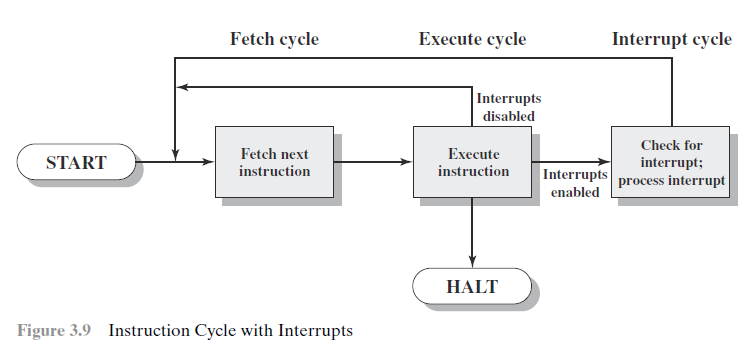
An Interrupt Cycle is appended to the instruction cycle following execution.
The processor evaluates pending interrupt signals:
If no interrupt is pending, execution proceeds to the standard Fetch cycle for the next sequential instruction.
If an interrupt is pending, the processor performs the following steps:
Suspends execution of the current program and saves its current context (saving the Program Counter address and processor status flags).
Sets the Program Counter to the entry address of the OS Interrupt Handler program.
Proceeds to the Fetch cycle to fetch and execute the first instruction of the interrupt handler routine.
Input/Output (I/O) Management and Data Transfer Modes
I/O Resource Management:
The Operating System issues commands to devices, handles hardware interrupts/errors, and regulates resource access among competing processes to prevent device conflicts and deadlocks.
Hardware Device Controllers:
Motherboard or expansion card components that bridge the CPU and physical hardware devices.
Translates CPU instructions against an internal command list and forwards commands directly to the hardware.
Specific Controller Types:
Keyboard Controller: Controls keyboard and PS/2 mouse devices.
DMA Controller: Manages Direct Memory Access operations.
Network Adaptor Controller: Manages Network Interface Cards (NICs).
IDE Controller: Controls EIDE hard disks and CD/DVD drives.
Graphics Adaptor: Controls display output devices (monitors, projectors).
USB Controller: Manages connected USB devices.
Interrupt Controller Operations:
Special motherboard component that manages and prioritizes device Interrupt Requests (IRQs) before forwarding them to the CPU.
Devices raise IRQs associated with unique IRQ numbers.
Priorities are assigned hierarchically: lower IRQ numbers correspond to higher priority levels.
Processor-I/O Interfacing Approaches:
Memory-Mapped I/O: A dedicated portion of system memory address space is mapped directly to I/O devices. The processor uses identical read/write instructions for system RAM and peripheral I/O access.
Port-Mapped I/O: Implements a completely separate address space independent of system memory, using Port Numbers as addresses. Requires specialized, distinct I/O instruction codes.
Three Modes of I/O Execution:
Programmed I/O: The processor directly controls the I/O operation (senses device status, sends read/write commands, transfers data). The CPU must wait/poll until the I/O operation completes, wasting processor time.
Interrupt-Driven I/O: The CPU issues an I/O command, continues executing other background instructions, and is interrupted by the I/O module once data transfer completes.
Direct Memory Access (DMA): Eliminates CPU intervention by enabling direct data exchange between memory and I/O modules.
Requires a dedicated DMA Controller module on the system bus capable of mimicking the processor.
Operates during unused CPU bus cycles or forces temporary CPU suspension (termed cycle stealing).

Internal DMA Components: Data Count Register, Data Register, Address Register, and Control Logic (driving Data lines, Address lines, DMA Request, DMA Acknowledge, Interrupt, Read, and Write signals).
Instruction Set Architectures: CISC vs. RISC
Definition of Instruction Set Architecture (ISA):
Represents the formal interface boundary ("contract") between hardware and software.
Defines operations, modes, storage locations, and exact invocation interfaces supported by hardware.
Does NOT guarantee underlying microarchitectural implementations, execution speed, or power consumption metrics.
Key Architectural Innovations:
Family Concept: Decouples ISA definition from physical implementation, enabling varying performance/cost tiers.
Microprogrammed Control Unit: Utilizes fast control memory to implement complex ISAs efficiently.
Cache Memory: High-speed buffer memory bridging CPU-RAM speed gaps.
Pipelining: Introduces parallel execution stages into sequential instruction streams.
Multiple Processors: Combines multiple execution cores or processors.
Complex Instruction Set Computer (CISC):
Design Motivation: Supports high-level programming languages, simplifies compiler design via multi-operation instructions, and reduces program code size.
Characteristics: Rich instruction set where a single instruction can load operands from memory, perform calculations, and store results back to memory. Instructions require multiple clock cycles to complete.
Drawbacks: Provides little to no savings in compiled program size while making the Control Unit excessively complex and reducing silicon space available for CPU registers (e.g., x86).

Relative Code Size Empirical Data (Table 13.6):
RISC I: PATT82a (11 C Programs) = , KATE83 (12 C Programs) = , HEAT84 (5 C Programs) =
VAX-11/780: PATT82a = , KATE83 = , HEAT84 = N/A
M68000: PATT82a = , KATE83 = N/A, HEAT84 =
Z8002: PATT82a = , KATE83 = N/A, HEAT84 =
PDP-11/70: PATT82a = , KATE83 = , HEAT84 = N/A
Reduced Instruction Set Computer (RISC):
Characteristics: Smaller, streamlined instruction set; simple fixed instruction formats; simple addressing modes; register-to-register execution model; executes one instruction per clock cycle.
Advantage: Simple control logic frees up silicon die space, enabling large internal register files (e.g., ARM processors).
Detailed ISA Architectural Comparison (Table 13.1):
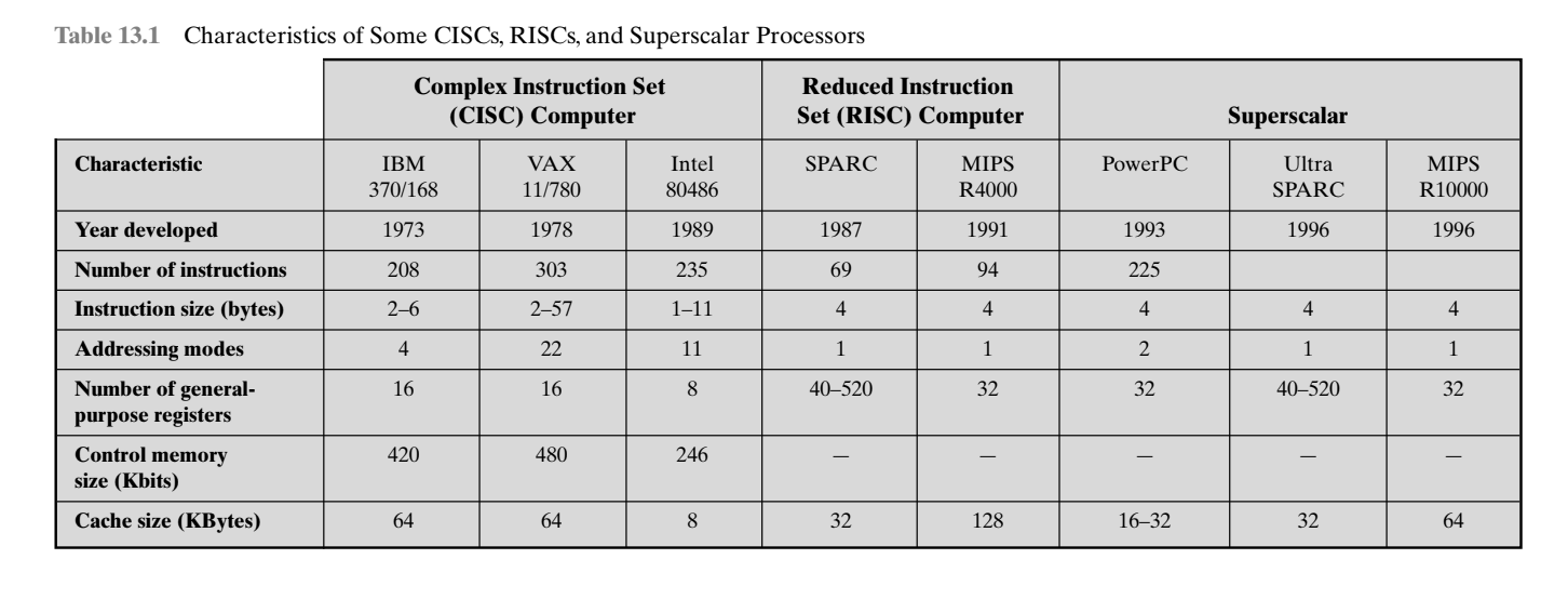
CISC Processors:
IBM 370/168 (1973): instructions; instruction size ; addressing modes; general-purpose registers; control memory; cache.
VAX 11/780 (1978): instructions; instruction size ; addressing modes; general-purpose registers; control memory; cache.
Intel 80486 (1989): instructions; instruction size ; addressing modes; general-purpose registers; control memory; cache.
RISC Processors:
SPARC (1987): instructions; instruction size ; addressing mode; general-purpose registers; no microcode control memory (-$); cache.
MIPS R4000 (1991): instructions; instruction size ; addressing mode; general-purpose registers; no microcode control memory (-$); cache.
Superscalar Processors:
PowerPC (1993): instructions; instruction size ; addressing modes; general-purpose registers; no microcode control memory (-$); cache.
Ultra SPARC (1996): Instruction count unspecified; instruction size ; addressing mode; general-purpose registers; no microcode control memory (-$); cache.
MIPS R10000 (1996): Instruction count unspecified; instruction size ; addressing mode; general-purpose registers; no microcode control memory (-$); cache.
Addressing Modes, Instruction Categories, and Processor Families
Four Core Addressing Modes:
Absolute Addressing Mode: Explicitly specifies the exact memory location containing the value to read or write.
Absolute Indexed Addressing Mode: Computes a memory address by adding a fixed base address (encoded in the instruction) to an offset held in a register.
Indirect Indexed Addressing Mode: Reads a 2-byte memory address from main memory to serve as a base address, then computes the effective target address.
Immediate Addressing Mode: Encodes the operand value directly within the instruction word itself.
Detailed Instruction Categories:
Memory Load and Store: Reads data values from memory into CPU registers, or writes register data back to system memory.
Register-to-Register Data Transfer: Copies data values directly from a source register to a destination register.
Stack Instructions: Transfers data between registers and the stack pointer register (); used for stack initialization and handling interrupt state flags.
Arithmetic Instructions: Supports addition and subtraction operations.
Logical Instructions: Performs bitwise AND, OR, and XOR operations between registers and operands.
Branching Instructions: Loads target addresses into the Program Counter () register to redirect program flow.
Subroutine Call and Return: Pushes the return address onto stack and branches to a subroutine; return instructions restore execution at
Processor Flag Instructions: Explicitly sets or clears status flags inside the CPU status register.
Interrupt-Related Instructions: Sets/clears flags, triggers software interrupts, or returns from interrupt service routines.
No Operation (NOP): Increments the Program Counter () register to the next instruction without performing any operational action; used for debugging and timing delays.
Major Processor Architectures:
x86 Architecture:
Originated with the Intel 8086 CPU and Intel 8088 variant.
Dominates personal computer, laptop, workstation, server, and TOP500 supercomputer cluster markets.
Supported OS Environments: DOS, Windows, Linux, FreeBSD, NetBSD, OpenBSD, Solaris, and macOS.
Features variable instruction lengths, CISC design emphasis, and extensive backward compatibility.
x86_64 (x64 / AMD64 / Intel 64):
64-bit extension of x86 standard originally designed by AMD in 2000; adopted by AMD, Intel, and VIA.
Supports a theoretical maximum memory address space of () of virtual and physical memory.
IA-64 (Itanium Architecture):
64-bit ISA developed jointly by Hewlett-Packard (HP) and Intel.
Based on Explicit Instruction-Level Parallelism (ILP/EPIC), relying on the compiler to organize parallel instruction execution rather than hardware superscalar checks.
Designed to surpass RISC processing limits (~1 instruction per cycle limits); supports hardware multithreading (2 thread contexts per core) and hardware virtualization.
ARM Architecture:
Originally Acorn RISC Machine, currently Advanced RISC Machine (ARM Holdings, Cambridge, UK).
RISC design requiring fewer transistors than CISC processors, significantly reducing cost, power consumption, and heat dissipation. Ideal for battery-powered portable devices.
Over ARM processors manufactured as of 2017 (most produced ISA in history).
ARMv8-A introduces 64-bit address space and 64-bit arithmetic execution.
SPARC Architecture:
Scalable Processor Architecture, developed by Sun Microsystems.
Minimalist RISC design with few opcodes aiming for ~1 instruction per clock cycle execution. Killed off by Oracle in 2017.
Supported OS Environments: SunOS, Solaris, OpenSolaris, FreeBSD, OpenBSD, NetBSD, and Linux.