Memory System Design Notes
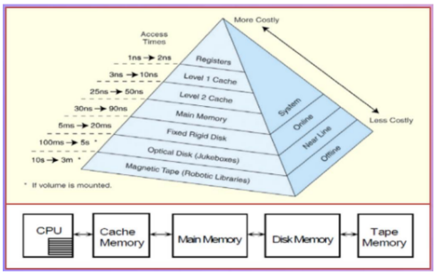
The memory hierarchy consists of different types of memory organized according to speed and cost.
Hierarchy Levels:
Registers (1ns)
Level 1 Cache (2ns - 10ns)
Level 2 Cache (10ns - 25ns)
Main Memory (50ns - 100ns)
Fixed Rigid Disk (5ms)
Optical Disk (20ms)
Magnetic Tape (hundreds of ms to a few seconds)
Key Concept: Faster memory is more costly and has less capacity. Slower memory is less costly and has larger capacity.
Objectives of a Memory Hierarchy
To minimize execution time of executing programs.
To maximize the throughput of the computer.
To minimize response time.
Registers
Small, fast memories located within the CPU used for specific purposes.
Kinds of Registers:
General Purpose Registers: Holds frequently needed data and intermediate results.
AX (Accumulator): Holds arithmetic operations.
BX (Base): Holds address of a procedure or variable.
CX (Counter): Holds count for loops or shift instructions.
DX (Data): Holds high bits of multiplication results and performs division.
Segment Registers: Base locations for program instructions, data, and stack.
CS (Code Segment): Base location for executable instructions.
SS (Stack Segment): Base for the stack.
DS (Data Segment): Default base for variables.
ES (Extra Segment): Additional base for variables.
Index Registers: Offset of data currently executed by the CPU.
BP (Base Pointer): Offset for stack-based variables.
SP (Stack Pointer): Offset for the top of the stack.
Source Index (SI) and Destination Index (DI): Used for string operations.
Instruction Pointer (IP): Offset for the next instruction.
Flags: Indicate CPU status or results of operations.
Control Flags: IF, TF, DF.
Status Flags: CF, OF, SF, ZF, AF, PF.
Cache Memory
Small, fast temporary storage for frequently accessed instructions and data.
Acts as a buffer between the CPU and main memory.
Access Times: L1 Cache (4ns), L2 Cache (15-20ns), L3 Cache (between L1 and main memory).
Cache Types
Level 1 Cache: 8 KB to 64 KB, on the processor.
Level 2 Cache: 64 KB to 2 MB, on motherboard or expansion card.
Level 3 Cache: 2 MB to 256 MB, between processor and main memory.
Main Memory
Internal or Main Memory (RAM): Fast and larger than cache.
Holds program code and data.
Types of RAM:
Static RAM (SRAM): Retains values indefinitely; faster but more expensive.
Dynamic RAM (DRAM): Must be refreshed regularly; slower; cheaper.
SDRAM: Synchronized with CPU clock.
DDR SDRAM: Transfers data on both clock edges.
Read Only Memory (ROM)
Non-volatile; used for critical system information.
Types of ROM:
PROM: Programmable once.
EPROM: Erasable with UV light.
EEPROM: Electronically erasable; supports updates.
Flash Memory: Non-volatile memory that requires block erasure.
Disk Memory
Magnetic Disks: Circular platters where data is magnetically recorded.
Hard Disks: Rigid plates that spin (5400 to 7200 RPM).
Floppy Disks: Portable and inexpensive.
Optical Disks: Read with lasers; includes CD, DVD, BluRay.
Tape Memory: Slow access; used in archival storage.
Cache Memory Organization
Direct Mapped Cache: Each address has a specific place in cache; simple and commonly used.
Fully Associative Cache: Searches entire cache; complex but performs well.
Set Associative Cache: Combination of both types for better performance.
Analyzing Cache Effectiveness
Hit: Data found at given memory level.
Miss: Data not found.
Hit Rate: Percentage of successful data retrieval.
Miss Rate: Percentage of retrieval failures.
Miss Rate Calculation:
Hit Time: Time to access data.
Miss Penalty: Time to process a miss, including data retrieval.