Semiconductor Diode
Semiconductor Diode Materials
Semiconductor diodes are electronic components that play a crucial role in the field of electronics by allowing the flow of electric current in one direction while restricting it in the opposite direction. The materials used in semiconductor diodes are carefully chosen to exploit the unique properties of semiconductors.
The most common types of semiconductor diodes, such as the P-N-junction diode, are typically made from materials like silicon (Si) and germanium (Ge). These materials are semiconductors, meaning they have electrical conductivity between that of conductors (like metals) and insulators (like rubber).
In the case of a P-N-junction diode, it consists of two semiconductor regions: one doped with a specific type of impurity to create an excess of electrons (n-type) and the other doped with a different impurity to create a deficiency of electrons, or "holes" (p-type). The interface between these two regions forms the P-N-junction, which is crucial to the diode's operation.
Silicon is the most widely used material for semiconductor diodes due to its abundance, stability, and well-understood manufacturing processes. Germanium, though less common, was historically used and is still employed in some niche applications.
The choice of semiconductor material influences the diode's electrical characteristics, such as its forward voltage drop, temperature sensitivity, and maximum operating frequency. Advances in materials science and semiconductor technology continue to contribute to the development of more efficient and specialized diodes for various applications in electronics and telecommunications.
Semiconductor Diode
A semiconductor diode is a P-N junction diode. It is a two terminal device that conducts current only in one direction.
Semiconductor Diode Symbol
P-N junction is denoted by this symbol. The arrow indicates the permissible direction of the current.
P-N Junction Diode Under Forward Bias
Under forward bias, the electric field created by the applied voltage assists the majority charge carriers (holes in the P-type and electrons in the N-type) in moving towards the junction. In other words, the applied voltage reduces the potential barrier at the junction, allowing the charge carriers to overcome it and cross from one side to the other. As electrons move from the N-type to the P-type and holes move from the P-type to the N-type, they recombine near the junction. This process leads to the creation of a region near the junction with reduced charge carriers, known as the depletion region. As a result, the depletion region at the junction becomes narrower, reducing the barrier for the flow of charge carriers.
The P-N junction diode exhibits low resistance, allowing a significant current pass through. The diode conducts electricity easily, and this forward conduction state is essential for various electronic applications such as rectification in power supplies and amplification in semiconductors devices like transistors. The voltage-current characteristic curve of a P-N junction diode under forward bias shows an exponential relationship indicating a rapid increase in current with a slight increase in voltage.
P-N Junction Diode Under Reverse Bias
When a reverse bias voltage is applied, the positive terminal of the voltage source connects to the N-type material, and the negative terminal connects to P-type material resulting a increase of width in depletion region at the junction. The external voltage works against the built-in potential, causing the electrons in the N-type material to move away from the junction and the holes in P-type material to move away as well.
Under reverse bias, the P-N junction exhibit several characteristics. First, the width of the depletion zone increases, leading to a reduction in the electric current flowing through the diode. Second, the reverse bias increases the potential energy barrier, making it more difficult for charge carriers to overcome and traverse the junction. As a result, the flow of current is significantly limited, and the diode acts as an insulator.
In a reverse-biased P-N junction diode:
Depletion Region Widening: The external electric field created by the reverse bias causes the depletion region to expand. This occurs because the negative potential on the N-type side repels electrons away from the junction, and the positive potential on the P-type side repels holes away from the junction.
Reduced Current Flow: The widened depletion region acts as a barrier to the flow of charge carriers, reducing the current through the diode. As a result, the reverse current (also called leakage or saturation current) becomes very small.
High Resistance: The reverse-biased P-N junction exhibits high electrical resistance, preventing the flow of current in the reverse direction.
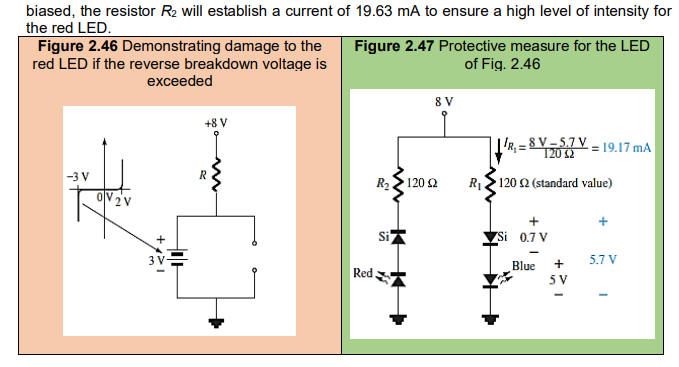
Breakdown: If the reverse bias voltage exceeds a certain critical value, known as the breakdown voltage or reverse breakdown voltage, the P-N junction may experience a breakdown. This breakdown can lead to a sudden increase in reverse current and can cause the diode to conduct in the reverse direction.
Semiconductor Diode Characteristics
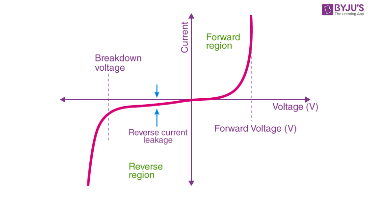
Forward Bias:
When a positive voltage is applied to the p-type (anode) and a negative voltage to the n-type (cathode) of the diode, it is said to be in forward bias.
In this mode, the diode conducts current, and the voltage across the diode increases slowly at first and then more rapidly.
Reverse Bias:
When a negative voltage is applied to the p-type and a positive voltage to the n-type, the diode is in reverse bias.
In this mode, the diode does not conduct appreciable current, and there is a small reverse leakage current.
Threshold Voltage (Forward Voltage Drop):
The voltage at which the diode begins to conduct significantly in the forward direction is known as the threshold voltage or forward voltage drop.
Different types of diodes have different threshold voltages; for silicon diodes, it is typically around 0.7 volts.
Reverse Breakdown Voltage:
Beyond a certain reverse bias voltage, the diode experiences a sudden increase in reverse current, known as breakdown.
The reverse breakdown voltage is an important parameter and can be either a specified value for normal operation or a protection mechanism.
Diode Current-Voltage (I-V) Characteristics:
The relationship between the voltage across a diode and the current flowing through it is represented by the diode's current-voltage characteristics.
The ideal diode equation is often used to describe the behavior of a diode under different bias conditions.
Temperature Dependence:
The characteristics of a semiconductor diode are influenced by temperature. Generally, the forward voltage drop decreases with increasing temperature, while reverse leakage current may increase.
Resistance Levels
As the operating point of a diode moves from one region to another the resistance of the diode will also change due to the nonlinear shape of the characteristic curve. It will be demonstrated in the next few paragraphs that the type of applied voltage or signal will define the resistance level of interest. Three different levels will be introduced in this section, which will appear again as we examine other devices. It is therefore paramount that their determination be clearly understood.
DC or Static Resistance
DC or static resistance is the resistance offered by a diode when a direct current (DC) is applied to it. It is measured by taking the ratio of the DC voltage across the diode to the DC current flowing through it. DC or static resistance depends on the operating point of the diode, which is the combination of the DC bias voltage and current. DC or static resistance can be calculated by using the Shockley diode equation, which relates the diode current to the diode voltage. The formula for DC or static resistance is:
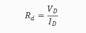
where VD and ID are the DC diode voltage and current, respectively.
In general, therefore, the higher the current through a diode, the lower is the DC resistance level.
AC or Dynamic Resistance
The DC resistance of a diode is independent of the shape of the characteristic in the region surrounding the point of interest.
AC or dynamic resistance is the resistance offered by a diode when an alternating current (AC) is applied to it. It is different from the static or DC resistance, which is the resistance when a direct current (DC) is applied to the diode. AC or dynamic resistance depends on the operating point of the diode, which is the combination of the DC bias voltage and current. AC or dynamic resistance can be calculated by using the Shockley diode equation, which relates the diode current to the diode voltage. The formula for AC or dynamic resistance is:
where ΔV and ΔI are the small changes in the diode voltage and current due to the AC signal, n is the ideality factor of the diode, VT is the thermal voltage, and ID is the DC diode current.
Average AC Resistance
Average AC resistance is a term that describes the effective resistance of a diode when an alternating current (AC) is applied to it. It is different from the static or DC resistance, which is the resistance when a direct current (DC) is applied to the diode. Average AC resistance is calculated by dividing the peak voltage across the diode by the peak current through it. The formula for average AC resistance is:
where Vp and Ip are the peak diode voltage and current, respectively. Average AC resistance is useful for determining the average power dissipated by the diode in an AC circuit.
As with the DC and AC resistance levels, the lower the level of currents used to determine the average resistance, the higher is the resistance level.
Diode Equivalent Circuits
An equivalent circuit is a combination of elements properly chosen to best represent the actual terminal characteristics of a device or system in a particular operating region.
Diode equivalent circuits are simplified models that represent the behavior of a diode in a circuit. They can be used to analyze the voltage, current, and power of the diode and the circuit. There are different types of diode equivalent circuits, depending on the level of accuracy and complexity required. Some of the common diode equivalent circuits are:
Ideal diode model: This is the simplest model that assumes the diode has zero resistance when it is forward biased and infinite resistance when it is reverse biased. It can be represented by a switch that is closed when the diode is on and open when the diode is off. This model is useful for qualitative analysis and understanding the basic operation of the diode, but it does not account for the voltage drop, the leakage current, or the nonlinearity of the diode.
Piecewise-linear model: This is a more realistic model that approximates the diode characteristics by straight-line segments. It can be represented by a battery, a resistor, and an ideal diode in series. The battery represents the voltage drop across the diode when it is on, the resistor represents the dynamic resistance of the diode, and the ideal diode represents the switch behavior of the diode. This model is useful for quantitative analysis and designing the circuit, but it still ignores some of the nonlinear effects of the diode.
Exponential model: This is the most accurate model that uses the Shockley diode equation to describe the relationship between the diode voltage and current. It can be represented by a current source and an ideal diode in parallel. The current source represents the photocurrent or the leakage current of the diode, and the ideal diode represents the exponential behavior of the diode. This model is useful for detailed analysis and simulation of the circuit, but it is more complex and requires numerical methods to solve.
The simplified equivalent circuit for a diode is a model that approximates the behavior of a real diode by using a battery and an ideal diode. The battery represents the threshold voltage that must be exceeded to turn on the diode, and the ideal diode represents the unidirectional conduction of the diode. The simplified equivalent circuit is useful for analyzing circuits that involve diodes, especially when the forward resistance and the reverse saturation current of the diode can be ignored. The simplified equivalent circuit for a silicon diode is shown below:
+0.7V
| |
| | +----->|----+
| | | |
| | | R
| | | L
| | | |
| | +------+----+
| |
+--+
The battery has a voltage of 0.7 V, which is the typical turn-on voltage for a silicon diode. The ideal diode has an arrow that indicates the direction of the forward current. When the diode is forward biased, the voltage across the diode is approximately equal to the battery voltage, and the current through the diode is determined by the external circuit. When the diode is reverse biased, the ideal diode acts as an open circuit, and the current through the diode is zero. The simplified equivalent circuit can be used to calculate the voltage and current in the load resistor RL, as well as the power dissipated by the diode and the load. For example, if the applied voltage is 10 V and RL is 1 kΩ, the current through the diode and the load is:
I = (10 V - 0.7 V) / 1 kΩ = 9.3 mA
The voltage across the diode and the load is:
VD = 0.7 V
VL = 9.3 mA x 1 kΩ = 9.3 V
The power dissipated by the diode and the load is:
PD = VD x I = 0.7 V x 9.3 mA = 6.51 mW
PL = VL x I = 9.3 V x 9.3 mA = 86.49 mW
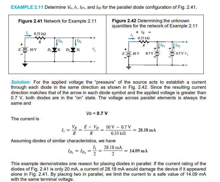
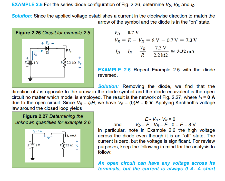
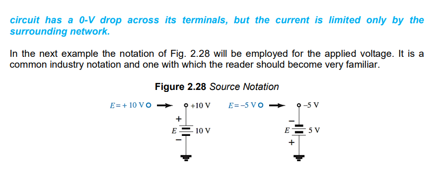
Series Diode Configurations

Parallel and Series-Parallel Configuration