Analog Design Chapter 2
Chapter 2: Amplifiers, Source Followers and Cascodes
Single Transistor Amplifiers
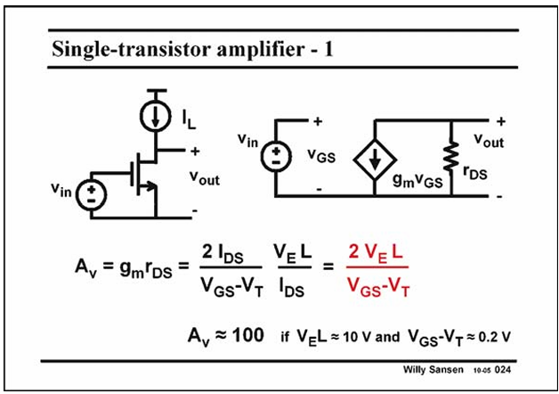
It is important to note that an amplifier is normally loaded by a DC current source. In this way the maximum gain can be obtained.
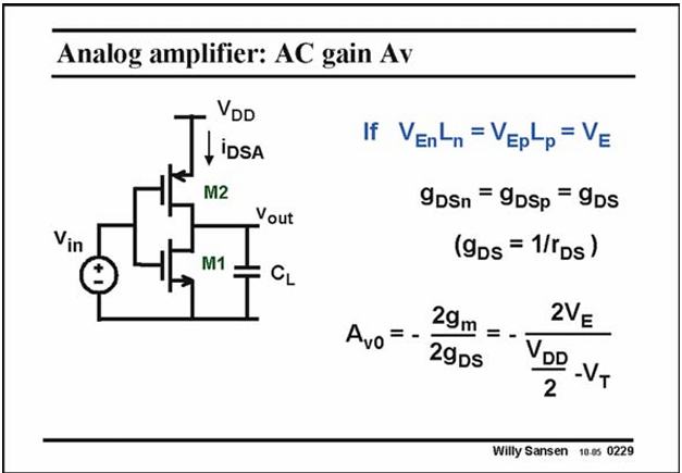
We take the take the value of VGS−VT as small as possible. A typical value is 0.15–0.2 V. We cannot go much lower as we then end up in the weak inversion region. The absolute value of the current and the trans conductance then become so small that the noise becomes too large.
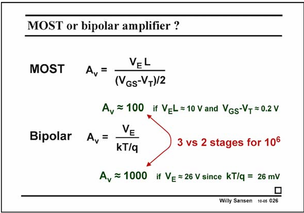
Even with a voltage gain of 100, three stages would be needed to obtain a voltage gain of 106, as is common in operational amplifiers. A bipolar transistor can provide the same gain in only two stages.
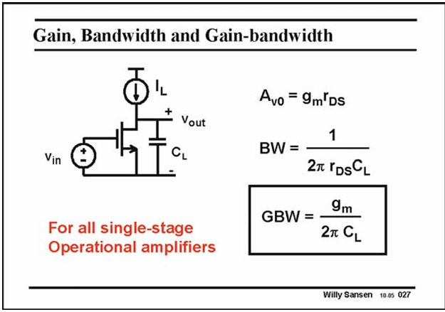
Figure of Merit (FOM), which quotes how much GBW can be obtained for a certain load capacitance and power consumption. Most opamps later on will have FOMs between 100 and 200, at least the better ones.
FOM = GBW*CL/Ids
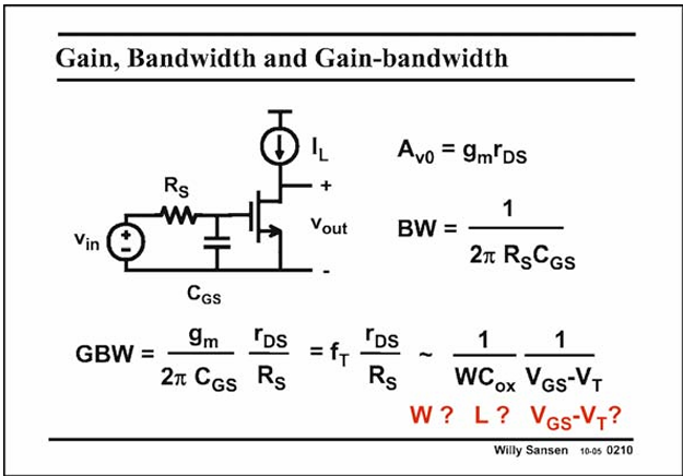
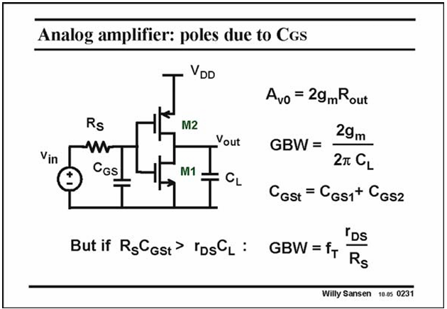
If no load capacitance is present, but a large input capacitance CGS , then the bandwidth is determined at the input.
In this case, the BW is simply given by the RC product at the input.
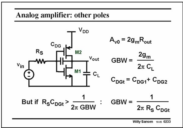
For high-frequency performance, it is not sufficient however to make fT large. Rather the product fT*rDS must be optimized, which is a technological challenge indeed!
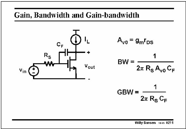
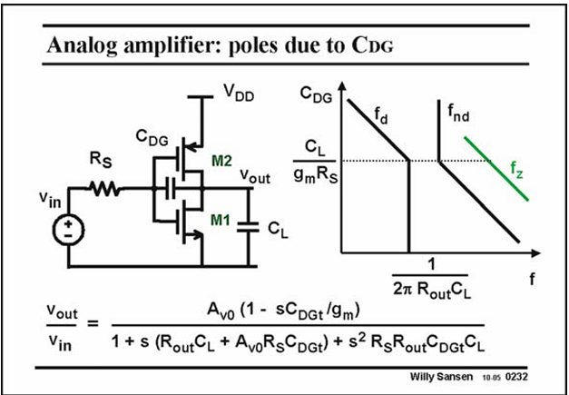
Finally, the third and final possible addition of a single capacitance to this circuit, is shown in this slide. It is a feedback capacitance CF from output to input. It is also called a Miller capacitance.
The GBW is now completely independent of any transistor parameters. This is expected!
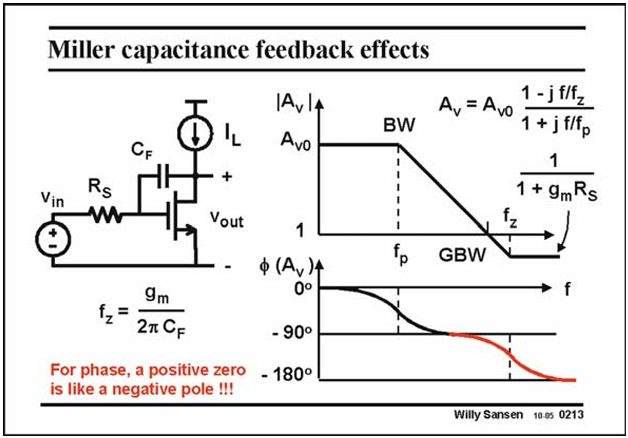
Actually, a Miller capacitance also causes a zero in the transfer characteristic.
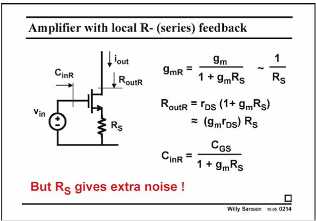
Quite often, local series feed back is applied to a single transistor amplifier, by means of a resistor RS.
For large resistors, the transconductance is reduced to 1/RS . It is independent of the current in contrast with gm.
A major effect is that the output resistance increases drastically. Indeed, it goes up by the same loop gain. An easy way to remember this expression is to take the series resistor RS , multiplied by the intrinsic transistor gain itself gm*RDS.
The input capacitance is decreased by the feedback. The larger the resistor RS , the smaller the input capacitance. If R S were replaced by a DC current source, the input capacitance would be negligible. Actually, the gain would be negligible as well.
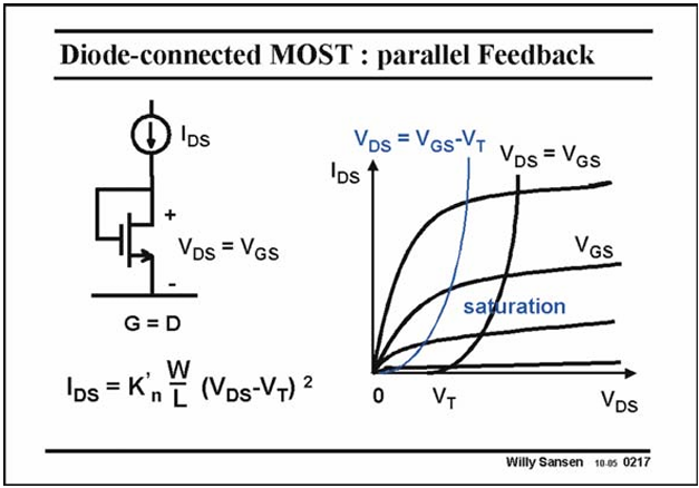
rds = 1/gm for diode connect structure above.
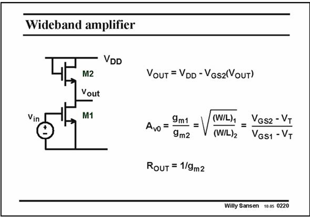
Suitable resistors are not always available. In a digital CMOS process, none of them can provide reason ably large resistance values. This is why many circuit schematics have been pro posed, using MOSTs as loads.
The gain is the ratio of the transconductances. It is small but fairly accurate as it is mainly set by the ratio of the transistor sizes.
Its main advantage is that no pMOSTs are used. This amplifier can achieve high bandwidths, also because the output impedance is quite small!
Its main disadvantage is that the DC output voltage is connected to the supply line over the VGS2 . Because of the body effect of transistor M2, this DC output voltage is not well defined. The biasing of the next stage may suffer from this.
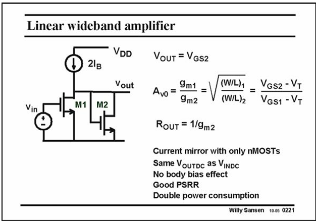
A better solution for the biasing is shown in this slide. There is a DC input voltage which gives rise to an equal DC output voltage. In this case the current is divided over both transistors and the gain is accurately given by the transistor size ratio or the VGS−VT ratio’s.
An additional advantage is that the circuit can easily be put in series with many more similar stages. This may be needed because the gain is small.
The body effect does not apply a role any more as all bulk contacts are grounded.
Again only nMOSTs are used for higher frequency performance.
The main drawback of this amplifier solution is that the current consumption is twice that of the previous circuit.
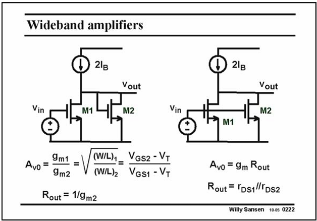
Compare two circuit above:
1st circuit: linearity + large bandwidth
2nd circuit: large gain
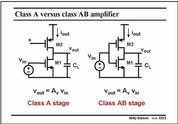
Class A stage: the DC current through transistors M1 and M2 does not change with the signal level.
Class AB: the currents in both transistors varies greatly depend on the input signal level.
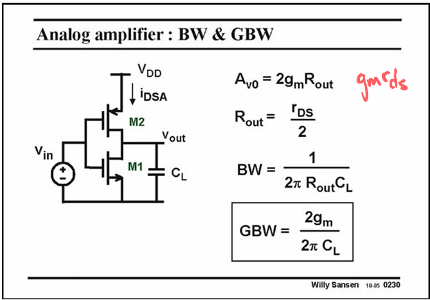
Compare with Common Source Amplifier:
Rout is smaller (a half)
BW and GBW is larger (double)