Analog Design Chapter 1
Chapter 1: Comparison of MOS and Bipolar Transistor
Model of MOS
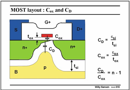
Both have dimensions F/cm−2
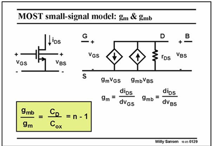
Normally CD is about one third of Cox.
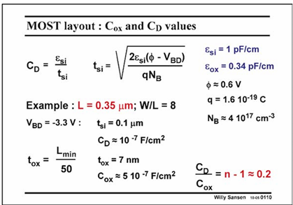
The ratio n−1 is then about 0.2. Most values of n are indeed between 1.2 and 1.5, depending on the value of tsi . Parameter n is thus never known accurately as it depends on biasing voltages.qqMOS as a Resistor
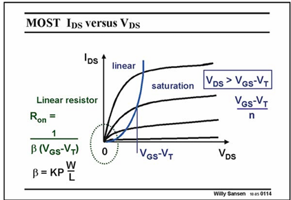
Where KP = µn*Cox
o µn ~ 600 Vs/cm2 OR µp ~ 250 Vs/cm2
o Cox = (δ(Si))/tox= (0.34 pF/cm)/(Lmin/50)
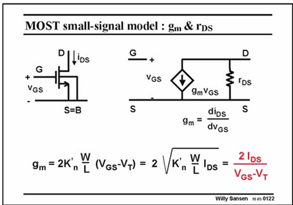
MOS as an Amplifier in Strong Inversion
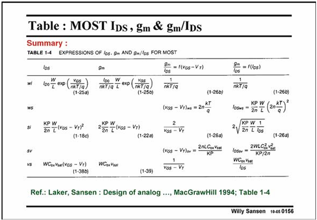
Gm: The last one is the best known. It does not contain any technological parameter such as K∞ and is the most precise one. This is why it is highlighted.
Rds:
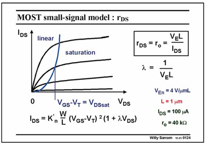
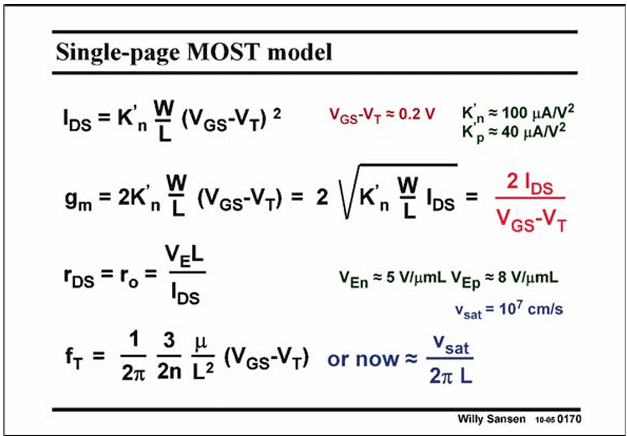
Parameter VE is the fourth technological parameter that we find: we have had up till now n, VT , KP and VE . Design parameters up till now are L and VGS−VT.
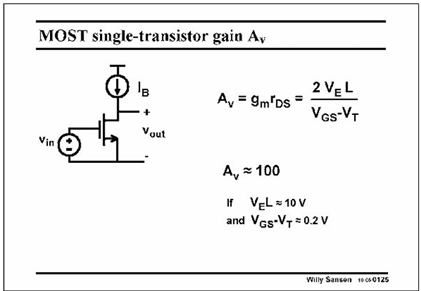
Deep submicron CMOS technologies only provide very limited gain. All possible circuit techniques will have to be used to provide large gain.
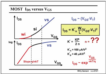
Transition Weak inversion - Strong inversion
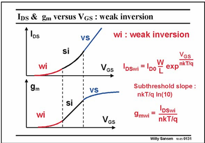
The scaling factor is nkT/q, which is very close to the one of a bipolar transistor where it is kT/q.
An approximate value of 70–80 mV is taken.
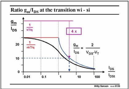
At lower currents the ratio gm/Ids is constant and is given by 1/(nkT/q). This value is about 1/40mV or 25 V−1. It is always smaller than for a Bipolar transistor where it is 1/26mV or 38 V-1 or about 40 V-1.
The ratio is a factor of about four. In other words, for the same transconductance, a bipolar transistor only needs four times less current than the MOST.
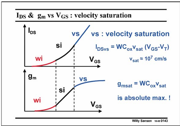
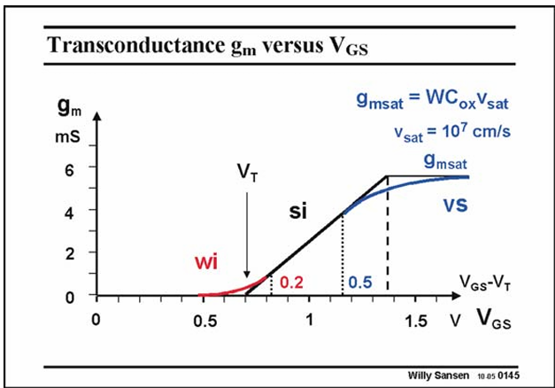
Transition Strong inversion - Velocity saturation
At the higher current end, several phenomena cause the current to become more linear versus VGS. One of the most important ones is velocity saturation.
This means that because of the high electric fields in the channel, all electrons move at maximum speed v sat . This speed is a result of a collision process of the electrons in the channel. Its average value is about 107 cm/s.
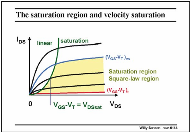
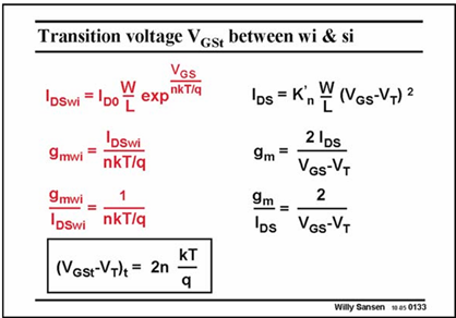
A MOST is in saturation when its VDS is sufficiently large or when VDS is larger than VDSsat , which equals VGS−VT.
In the saturation region the lower currents correspond to the weak inversion region.
The highest currents on the other hand correspond to the velocity saturation region.
The middle current region, which is shaded, corresponds to the region, which is characterized by the square-law model. These transistors operate in saturation and are in the square-law region.
Remember that we never want to enter the high-cur rent or velocity-saturation region.
Higher current Ids but doesn’t increase transconductance gm anymore.
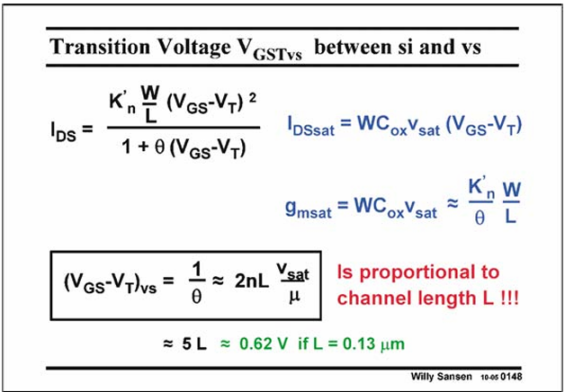
For typical values, this VGSTvs is just about 5L Volt with L in micrometer. It is clear that this transition voltage VGSTvs is not con stant, it decreases with decreasing channel length.
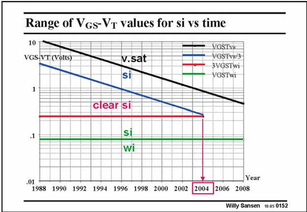
The region between the blue and red line is thus the range of VGST values in which a square law characteristic can easily be identified. As clearly shown, this region has just about disappeared.
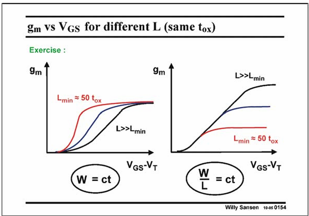
gm = un*Cox*W/L*(Vgs-Vt)
gmsat = W*Cox*vsat
Same tox so Cox doesn’t change and vsat = 10^7 cm/s
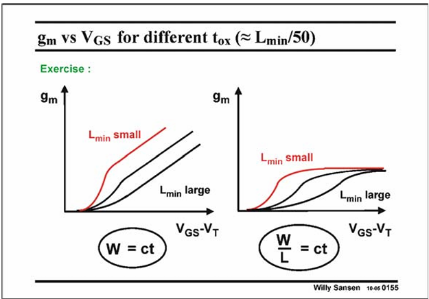
gm = un*Cox*W/L*(Vgs-Vt)
gmsat = W*Cox*vsat
Where Cox = 0.34/(Lmin/50) pF/cm and vsat = 10^7 cm/s
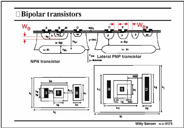
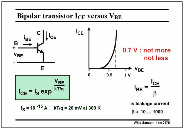
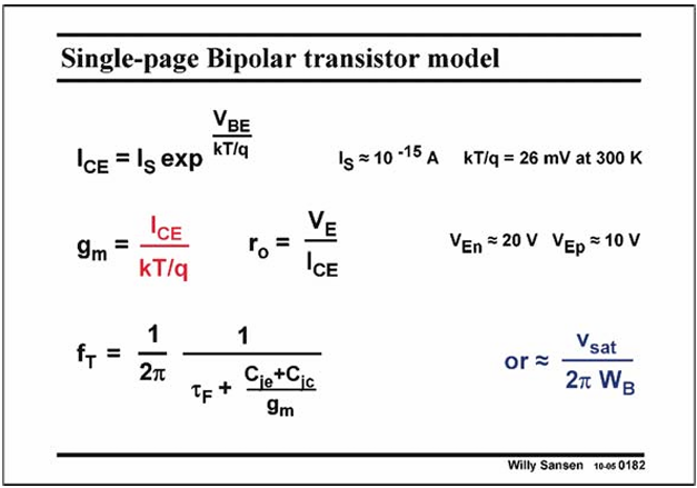
Model of Bipolar Transistor
Comparison of MOS and Bipolar Transistor
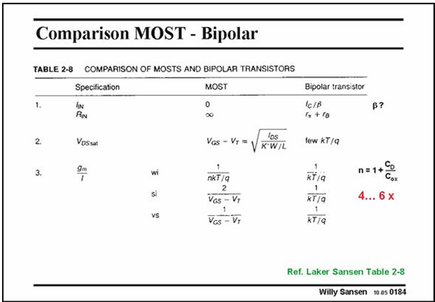
It is clear that the zero input current is a major advantage for a MOST. As a result, its input impedance is infinity. It is now possible to store a charge on a capacitance and read it with a nMOST.
In future nanometer technologies however, Gate current may flow in a similar way as for bipolar transistors. This is an enormous disadvantage for many circuits.
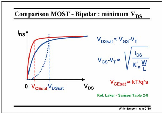
The second consideration is on the VDSsat . It is the minimum output voltage for which the MOST operates in saturation, exhibiting a large output resistance r o , and thus large gain.
The MOST operates in saturation, is little less than VGS−VT, which also sets the current depending on the transistor dimensions W and L.
For high-gain stages the VGS−VT is chosen to be small, such as 0.15–0.2 V.
For high-speed stages on the other hand, this VGS−VT may be as high as 0.5 V.
Bipolar transistors always exhibit a minimum output voltage of a few times kT/q. This is more of the order of magnitude of 0.1 V, whatever purpose the transistor is used for, high gain of high speed. This is clearly an advantage for the bipolar transistor. It is still the favorite device for very low supply voltages.
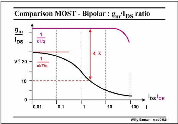
The gm/IDS ratio is also better with a bipolar transistor.
For a VGS−VT of 0.15–0.2 V, the gm/IDS ratio is around a factor of 4 better for a bipolar transistor than for a MOST.
For the same trans conductance, a bipolar transistor only requires 25% of the current of a MOST. This is a considerable advantage for portable applications, where battery power is expensive.