Fundamentals of Electronics Circuit
1: Introduction to Vacuum Tube Devices
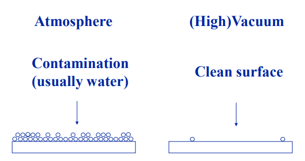
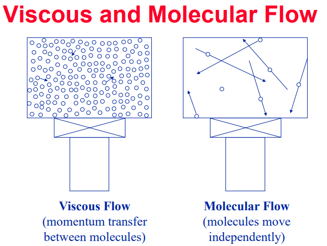
Why is a vacuum needed?
To move a particle in a (straight) line over a large distance.
To provide a clean surface.
Barometer – use to measure pressure
Mercury: 13.58 times heavier than water: Column is 13.58 x shorter: 10321 mm/13.58=760mm (= 760 Torr)
Pressure of 1 Standard Atmosphere:
760 Torr, 1013mbar at sea level, 0°C and 45°C Latitude
TORR - is a non-SI unit of pressure defined as 1/760 of an atmosphere. Named after Evangelista Torricelli, an Italian physicist and mathematician who discovered the principle of the barometer in 1644.
Gas Flow Conductance
Conductance is the reciprocal of the resistance and is measured in siemens or mhos.
Vacuum Tubes
A vacuum refers to a space where charged particles such as electrons, protons, neutrons and all other matter are absent. In other words, vacuum is nothing but the empty space.
Vacuum tube is an electronic device that controls the flow of electrons in a vacuum. It is also called as electron tube or valve.
History of Vacuum Tube
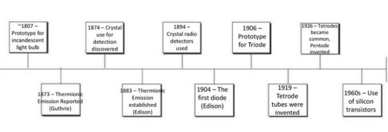
John Ambrose Fleming developed the first vacuum tube in 1904. Fleming’s diode allows the flow of electric current in only one direction (from cathode to anode) and blocks the electric current in another direction (from anode to cathode).
In 1906, American electrical engineer Lee De Forest invented Audion vacuum tube.
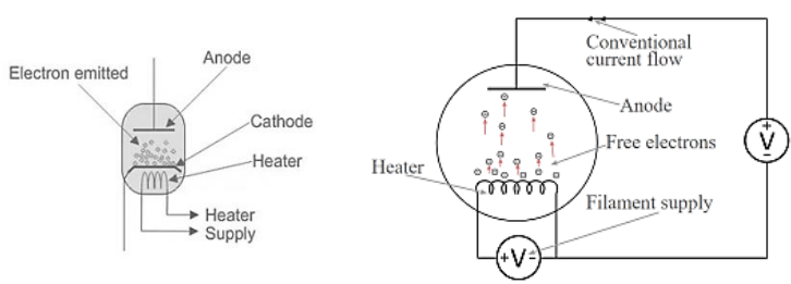
A vacuum tube consists of cathode (also called as filament), anode (also called as plate), and electrode (also called as grid).
Cathode is an electron emitter that emits the free electrons.
Anode is an electron collector that collects the free electrons.
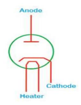
Directly heated and Indirectly heated Cathode Thermionic emission (archaically known as the Edison effect) is the flow of charged particles called thermions from a charged metal or a charged metal oxide surface, caused by thermal vibrational energy overcoming the electrostatic forces holding electrons to the surface.
If the heat or heating electric current is passed directly to the cathode that emits the free electrons, the cathode is said to be a directly heated cathode or directly heated emitter. In the directly heated cathode, the cathode itself is the heating element or filament. Hence, the heat required to emit the free electrons from the metal surface is less compared to the indirectly heated cathode.
Advantages of vacuum tubes:
Vacuum tubes are replaced easily.
Vacuum tubes can work at high temperatures without any damage.
Vacuum tubes produce superior sound quality.
Disadvantages of vacuum tubes:
Vacuum tubes are huge compared to semiconductor devices such as diodes, transistors, and integrated circuits.
Vacuum tubes generate more heat.
High voltages are required to operate the vacuum tubes.
Vacuum tubes consume more power.
High cost.
Failure rate is high.
Vacuum tubes occupy more space than the transistors.
Two Electrodes of Vacuum Diode
Vacuum diode is the simplest form of vacuum tube.
It consists of two electrodes, a cathode, and an anode or plate.
The cathode emits the free electrons. Hence, it is called as emitter.
The anode collects the free electrons. Hence, it is called as collector
Electrode is a conductor through which free electrons or electric current leaves or enters.
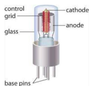
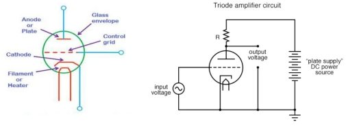
Vacuum Triode
To amplify the electrical signal, an extra electrode is required.
It has three electrodes: cathode, anode, and control grid.
The cathode is surrounded by a control grid, which is in turn surrounded by anode.
Control grid is placed more nearer to the cathode than anode to increase the electric current efficiently. Control grid will control the flow of electrons between the cathode and anode.
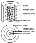
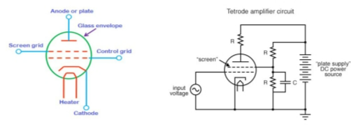
Vacuum Tetrode
Vacuum tetrode consists of four electrodes: cathode, anode, control grid, and screen grid. • The American physicist and electrical engineer Albert Wallace Hull invented the tetrode vacuum tube in 1926.
Screen grid is placed between the control grid and plate.
This grid is placed closer to the control grid than plate to reduce the capacitance efficiently.
Screen grid acts as an electrostatic shield to protect the control grid from the positive electric field or influence of the plate when its potential changes.
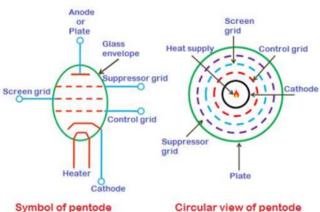
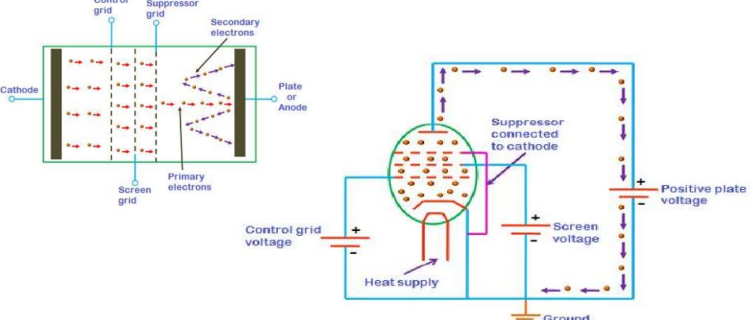
Vacuum Pentode
Vacuum pentode consists of five electrodes: cathode, control grid, screen grid, suppressor grid, and plate or anode. Bernard D. H. Tellegen invented the pentode in 1926.
The use screen grid in tetrode to reduce capacitance between the control grid and plate (anode). However, tetrodes have one drawback. When the screen grid voltage is greater than the plate voltage, the secondary electrons emitted from the plate are attracted to the screen grid. Because of this, the electric current flows in reverse direction (from plate to screen grid) which is undesirable.
This drawback can be overcome by placing an extra grid called suppressor grid in between screen grid and the plate. The suppressor grid repels secondary electrons towards anode or plate.
The suppressor grid is placed between the screen grid and plate. It is mainly used to repel the secondary electrons (emitted from anode) back to the anode.
It is internally connected to the cathode. Therefore, many free electrons are transmitted directly to the suppressor grid. Because of the gaining of excess electrons, suppressor grid acts as a negatively charged electrode and generates negative electric field. Therefore, it repels the secondary electrons (emitted from anode) back to anode.
Vacuum Tube Devices:
Cathode Ray Tubes
Vacuum Fluorescent Display
Vacuum Tubes Using Field Electron Emitters
Design uses a cold cathode in the form of a large area field electron source (field emitter array).
Include much and the ability to provide high power output at low power consumption.
Gas-Filled Tube
Operate by ionizing the gas with an applied voltage.
Ionizing is dependent on the pressure of the fill gas and geometry of the tube.
Nobel Gases:
Helium is used in helium-neon lasers
Neon used in fluorescent tubes with high power and short length. Ex. Industrial lighting tubes
2: Introduction to Semiconductors
Why we use Electronics?
Electronics are easy to move/control.
Easy to move/control electrons than real physical stuff.
Move information not things
phone, fax, internet
takes much less energy and money
Branch of Physics dealing with electrons, electronic devices and circuits.
Study of how to control the flow of electrons.
Deals with circuits made up of components that control the flow of electricity.
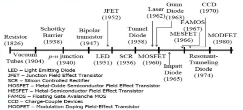
History of Semiconductor Devices
Atomic Structure
Basic Structure
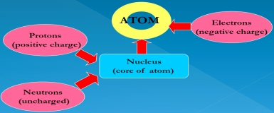
smallest particle of an element contains 3 basic particles.
Atom - Smallest unit of matter that retains all of the chemical properties or characteristics of an element.
3 Particles of an Atom:
Proton - Ernest Rutherford
Electron - JJ Thompson
Neutron - James Chadwick
this model was proposed by Niels Bohr in 1915.
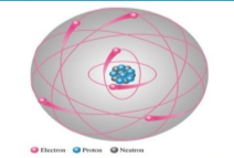 Electrons circle the nucleus that consists of protons and neutrons.
Atomic Number: Element in periodic table are arranged according to atomic number.
Atomic number = number of protons in nucleus.
Electron Shells and Orbits: Electrons near the nucleus have less energy than those in more distant orbits.
Each distance (orbits) from the nucleus corresponding to a certain energy level.
in an atom, the orbits are group into energy bands – shells.
Valence Electrons: electrons with the highest energy level exist in the outermost shell and loosely bound to the atom. The outermost shell – valence shell.
Electron in the valence shell called valence electrons.
Ionization: When atoms absorb energy (ex. Heat) – losing valence electrons called ionization.
Escape electron called free electron.
The Number of Electron in Each Shell: The maximum number of electrons (Ne) in each shell is calculated using the formula:
Ne = 2n²
n = number of shells
Ex. 2nd Shell
Ne = 2n² = 2(2) ² = 8
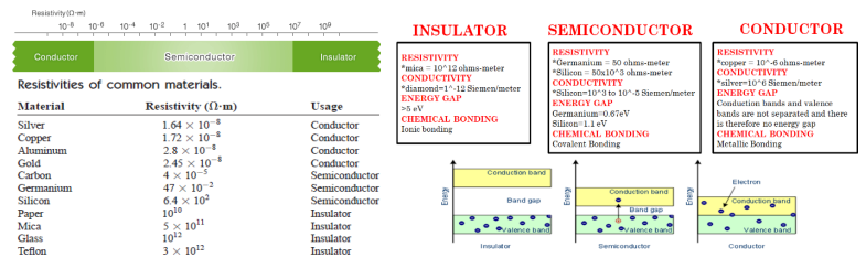
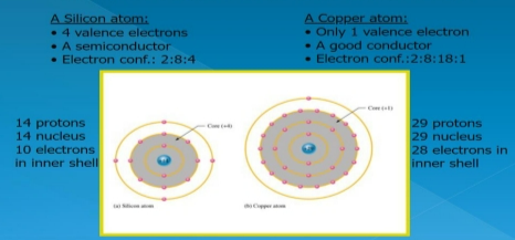
Semiconductors, Conductors, and Insulators
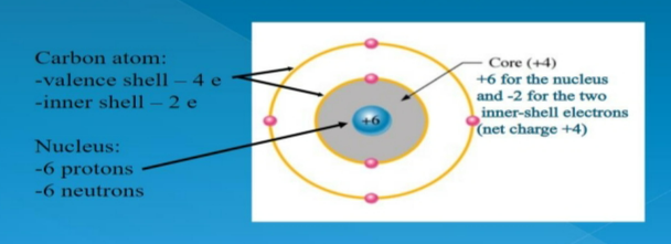
Atom can be represented by the valence shell and a core.
A core consists of all inner shell and the nucleus.
Conductors: Material that easily conducts electrical current.
the best conductors are single element material (ex. Copper, silver, gold, aluminum).
only one valence electron very loosely bound to the atom.
free electron.
Insulators: material does not conduct electrical current.
valence electrons are tightly bound to the atom.
very few free electrons.
Semiconductors: material between conductors and insulator in its ability to conduct electric current.
in its pure (intrinsic) state is neither a good conductor nor a good insulator.
most common semiconductor (ex. Silicon, germanium, and carbon) which contains four valence electrons.
Energy Bands
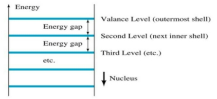
Energy Gap – the difference between the energy levels of any two orbital shells.
Band – another name for an orbital shell (valence shell = valence band).
Conduction Band – the band outside the valence shell where it has free electrons.
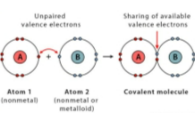
Covalent Bonding
Covalent bond is a chemical bond that involves the sharing of electrons to form electron pairs between atoms. These electron pairs are known as shared pairs or bonding pairs.
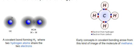
The binding arises from the electrostatic attraction of their nuclei for the electrons. It is responsible for holding the atoms together. Atoms share electrons so that they can obtain a stable electronic configuration following the octet rule. They are also known as molecular bonds.
Holding atoms together by sharing valence electrons.
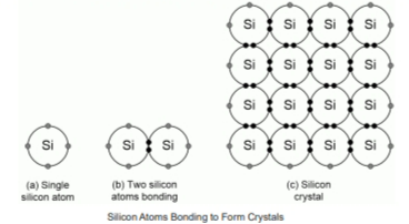
Rule of the Bonding:
The atoms are held together forming a solid substrate.
The atoms are all electrically stable, because their valence shells are complete.
The complete valence shells cause the silicon to act as an insulator-intrinsic (pure) silicon. In other word, it is a very poor conductor.
Covalent Bonding in an intrinsic (no impurities) or pure silicon crystal.
IONIC BONDING: Bond in which one or more electrons from one atom are removed and attached to another atom, resulting in positive and negative ions which attract each other.
METALLIC BONDING: Metallic bonding is the force of attraction between valence electrons and the metal atoms.
CONDUCTIVITY: a measure of its ability to conduct electricity.
ELECTRICAL CONDUCTIVITY: also called specific conductance.
the reciprocal of electrical resistivity and measures a material's ability to conduct an electric current.
It is commonly represented by the Greek letter σ (sigma).
The SI unit of conductivity is siemens per meter (S/m).
Resistance: the capacity of materials to impede the flow of current or, more specifically, the flow of electric charge.
the resistance of any material with a uniform cross-sectional area A depends on A and its length.
Resistivity (ρ): used when comparing the resistance level of materials and is measured in Ω-cm or Ω-m.
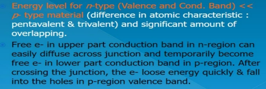
Conduction in Semiconductor
A pure silicon crystal with unexcited (no external energy such as heat) atoms. There are no electrons in the conduction band. This condition occurs only at a temperature of absolute 0K.
Conduction Electrons and Holes
Electrons – absorbs enough energy (thermal) to jump.
Electron-Hole Pair – a free electron and its matching valence band hole.
Recombination – when a conduction electron loses energy and fall back into hole in valence band.
Electron Current – The movement of electrons is one type of current in semiconductor.
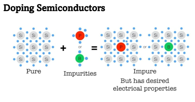
N-Type and P-Type Semiconductors
Doping – the process of creating N and P type materials.
By adding impurity atoms to intrinsic Si or Ge to improve the conductivity of the semiconductor.
2 Types of Doping
Trivalent (3 valence e)– a semiconductor added in P-Type material.
Ex. Al, Ga, B, In
Pentavalent (5 valence e)– a semiconductor added in N-Type material.
Ex. P, As, Sb, Bi
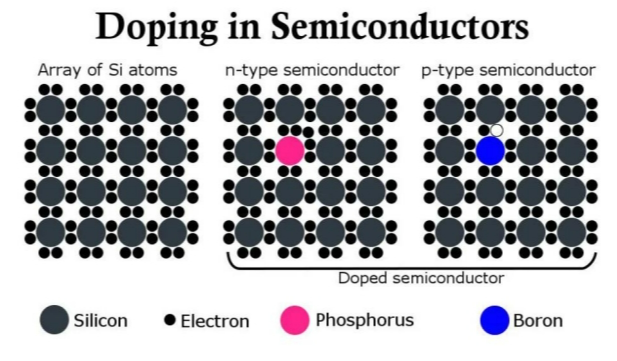
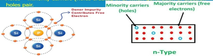
N-Type Semiconductor
Pentavalent impurities are added to Si or Ge, the result is an increase of free electrons.
1 extra electron becomes a conduction electron because it is not attached to any atom.
No. of conduction e can be controlled by the no. of impurity atoms.
Pentavalent atom gives up an electron – call a donor atom.
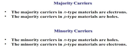
Current carries in n-type are electrons – Majority carriers.
Holes carries minority carriers.
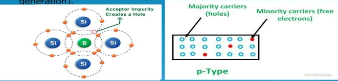
P-Type Semiconductor
Trivalent impurities are added to Si or Ge to increase number of holes.
Boron, Indium, and Gallium have 3 valence e form covalent bond with 4 adjacent silicon atoms. A hole created when each trivalent atom is added.
No. of conduction e can be controlled by the no. of trivalent impurity atoms.
Trivalent atom can take an electron – acceptor atom.
Current carries in p-type are holes – Majority carriers.
electrons carry minority carriers.
PN Junction Theory
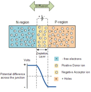
A PN-junction is formed when an N-type material is fused together with a P-type material creating a “PN Junction” or semiconductor diode.
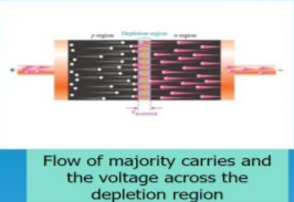
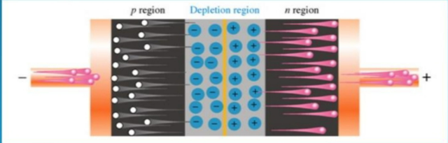
The charge density of the P-type along the junction is filled with negatively charged acceptor ions (NA), and the charge density of the N-type along the junction becomes positive. This charge transfer of electrons and holes across the PN junction is known as diffusion.
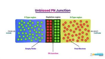
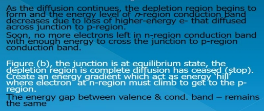
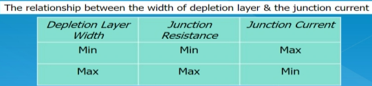
Depletion Layer
A PN-junction produced a “potential barrier” zone around the area of the junction as the donor atoms repel the holes and the acceptor atoms repel the electrons. The regions on either side of the junction now become completely depleted of any freer carriers in comparison to the N and P-type materials further away from the junction. This area around the PN Junction is now called the Depletion Layer.
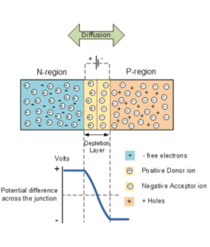
Potential Barrier
An electric field created by the diffusion process has created a “built-in potential difference” across the junction.
Typically, at room temperature the voltage across the depletion layer for silicon is about 0.6 – 0.7 volts and for germanium is about 0.3 – 0.35 volts.
Diode is a device that conducts current only in one direction.
N-type and p-type material becomes extremely useful when joined together to form a PN-junction – then diode is created.
Before the PN-junction is formed – no net charge (neutral) since no. of proton and electron is equal in both.
Barrier Potential (THRESHOLD VOLTAGE)
Electric Field – the forces between the opposite charges form a “field of forces”.
The electric field is a barrier to the free electrons in the n-region, need more energy to move an e- through the field.
Barrier Potential – potential difference of electric field across the depletion region is the amount of voltage required to move e- through the field.
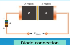
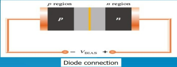
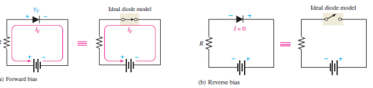
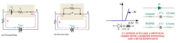
Biasing the Diode
No electron moves through the PN-junction at equilibrium state.
Bias – is a potential applied (dc voltage) to a PN-junction to obtain a desired mode of operation – control the width of the depletion layer.
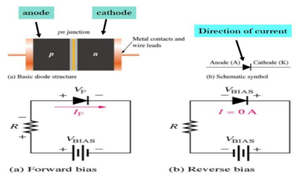
Forward Bias
Voltage source or bias connections are (+) to the p-region and (–) to the n-region.
the negative side of the bias voltage push the free electrons in the n-region -> PN-junction. Flow of free e- is called electron current.
the holes move to right toward the junction. This effective flow is called hole current.
the depletion region narrows.
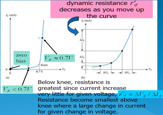
Effect of the Barrier Potential During Forward Bias
Free e- provided enough energy to climb the hill and cross the depletion region.
Dynamic Resistance – an additional small voltage drop occurs across the p and n region due to internal resistance of material.
Very small and can be neglected.
Reverse Bias
condition that prevent current through the diode.
voltage source or bias connection are (–) to the p-region and (+) to the n region.
current flow is negligible in most cases
depletion region widens than Forward bias.
Voltage-Current Characteristics of a Diode
Forward Current (If) – current when a forward bias voltage is applied.
Normal operation for a forward bias diode is above the knee of the curve.
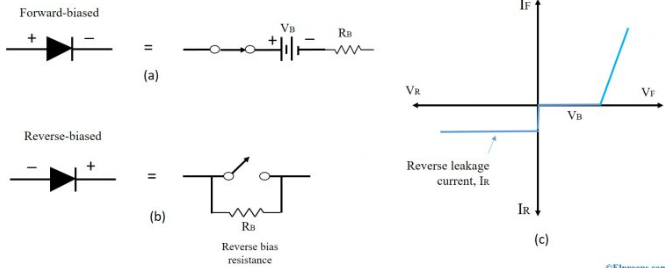
Diode Structure and Symbol
Diode Model
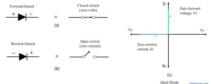
Ideal Diode Model
Closed (on) switch (FB), open (off) switch (RB).
Barrier potential, Dynamic resistance, and reverse current all neglected.
Assume to have zero voltage across diode when FB.
1st APPROXIMATION (IDEAL DIODE)
Diode is equivalent to a switch: Acts as a perfect conductor when forward biased and as a perfect insulator when reverse biased.
Used or ideal for troubleshooting
FORWARD ➢ Perfect Conductor (Zero Resistance) REVERSE ➢ Perfect Insulator (Infinite Resistance)
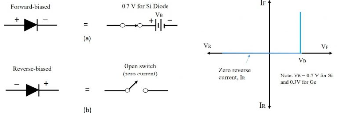
Practical Diode Model
Adds the barrier potential to the ideal switch model.
Rd is neglected.
2nd APPROXIMATION (PRACTICAL DIODE MODEL) Or Simplified Model or Constant Voltage Source
No current exist until source voltage overcome the barrier potential of the diode.
Excellent for troubleshooting and design analysis.
FORWARD ➢ When supply is greater than 0.7 V REVERSE ➢ When supply is less than 0.7 V
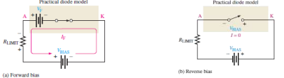
Complete Diode Model
Consist of BP, Rd, internal reverse resistance.
3rd APPROXIMATION (COMPLETE DIODE MODEL) Piecewise-Linear Model
Includes bulk resistance, RB.
After diode turns on, voltage increases linearly and proportionally with increase in current.
During conduction: VD = 0.7 V + IDRD
After diode turns on, Diode voltage increase LINEARLY and in proportion with the increase in current in current.
Bulk Resistance – ohmic resistance of semiconductor material.
Above Knee Voltage, current increase rapidly. Meaning, small voltage causes large increase in the diode current.
After the barrier potential has been overcome, all that impedes the current is the OHMIC RESISTANCE of the P and N region
BULK RESISTANCE is the sum of ohmic resistance (P and N)
3: Diodes
Diode Is a 2-terminal device.
Ideally conducts in only one direction.
A diode is a two-terminal electronic device that allows current to flow easily in one direction while presenting a high resistance in the reverse direction.
Anode – A, positive
Cathode – K, negative
Semiconductor Materials
Silicon (Si) -> 0.7V
Germanium (Ge) -> 0.3V
Gallium Arsenide (GaAs) -> 1.2V
Doping – the electrical characteristics of silicon and germanium are improved by adding in a process of doping.
N-Type – contain an excess of conduction band electrons.
N-Region – positive ion.
P-Type – contain an excess of valence band holes.
P-Region – negative ion.
Diode Operating Condition
No Bias
No external voltage is applied.
No current is flowing.
Only a modest depletion region exists.
Reverse Bias
External is applied across the PN- junction in the opposite polarity.
Causes the depletion region to widen.
Electrons in the n-type material area attracted toward the positive terminal of the Vs.
Holes in the p-type material are attracted toward the negative terminal of the Vs.
Forward Bias
External is applied across the PN- junction in the same polarity.
Causes the depletion region to narrow.
Electrons and holes are pushed toward the PN-junction.
Electrons and holes have sufficient energy to cross the PN-junction.
Zener Region
is in the diode’s reverse bias region.
the voltage that causes a diode to enter the Zener region of operation is called the Zener voltage.
BREAKDOWN REGION
Excessive Negative Voltage input to a diode.
Rapid Increase in Current due to avalanche.
Will destroy the diode.
Minimum reverse bias voltage that makes the diode conduct appreciably in reverse.
Maximum reverse bias voltage that can be applied without causing an exponential increase in the leakage current in the diode.
BREAKDOWN – is characterized by the rapid increase of the current under reverse bias.
BREAKDOWN VOLTAGE – is the corresponding applied voltage -typically 50V (can be found in the datasheet)
Once breakdown voltage is reach, a large minority carrier suddenly appears in Depletion Region, diode conduct heavily-due to avalanche effect.
AVALANCHE EFFECT
It is a form of electric current multiplication that can allow very large currents within materials which are otherwise good insulators.
occur at higher reverse voltage (at breakdown)
Peak Inverse Voltage or Peak Reverse Voltage
the maximum reverse voltage that won’t take a diode into the Zener region.
Temperature Effects
As temperature increase it adds energy to diode.
It reduces the required forward bias voltage for forward bias condition.
It increases the amount of reverse current in the reverse bias condition.
It increases maximum reverse bias avalanche voltage.
Germanium diodes are more sensitive to temperature variations than Si and GaAs.
Resistance Levels
DC (Static) Resistance
Specific applied DC voltage, the diode has a specific current, and a specific resistance.
AC (Dynamic) Resistance
FB Region:
The resistance depends on the amount of current in the diode.
The voltage across the diode is fairly constant (26mV for 25deg).
Internal resistance ranges from a typical 0.1 ohms for high power devices to 2 ohms for low power, general purpose diode. In some cases, internal resistance can be ignored.
RB Region:
Resistance is effectively infinite. The diode acts like an open.
Average AC Resistance
Can be calculated using the current and voltage values for two points on the diode characteristics curve.
Diode Capacitance
Reverse Bias:
The depletion layer is very large. The diode’s strong positive and negative polarities create capacitance. The amount of capacitance depends on the reverse voltage applied.
Forward Bias:
Storage capacitance or diffusion capacitance exists as the diode voltage increases.
Reverse Recovery Time (trr)
the time required for a diode to stop conducting once it is switched from forward bias to reverse bias.
Diode Checker
Ohmmeter – set on a low Ohms scale can be used to test a diode. The diode should be tested out of circuit.
Curve Tracer – displays the characteristics curve of a diode in the test circuit. This curve can be compared to the specifications of the diode from a data sheet.
4: Diode Circuit and Power Supply
Single Phase Rectification
Rectification is the process of linking an AC power supply to a connected DC load by means of solid-state semiconductor devices.
Rectification converts an oscillating sinusoidal AC voltage source into a constant current DC voltage supply by means of diodes, thyristors, transistors, or converters.
Rectifiers are one of the basic building blocks of AC power conversion with half-wave or full-wave rectification generally performed by semiconductor diodes.
Rectifier – an electrical device that converts alternating current (AC), which periodically reverses direction, to direct current (DC), which flows in only one direction.
The process is known as rectification, since it "straightens" the direction of current.
POWER SUPPLY UNIT – Circuit inside electronic equipment that converts the ac input voltage to an almost perfect dc output voltage. DC POWER SUPPLY converts the standard 220 V, 60 Hz AC voltage available at wall outlets into a constant DC voltage.
TRANSFORMER – Transformer changes ac voltages based on the turn’s ratio between the primary and secondary.
2 TYPES OF TRANSFORMER
STEP-UP TRANSFORMER
Example: 110V to 220V
STEP-DOWN TRANSFORMER – usual
Example: 220V to 110V
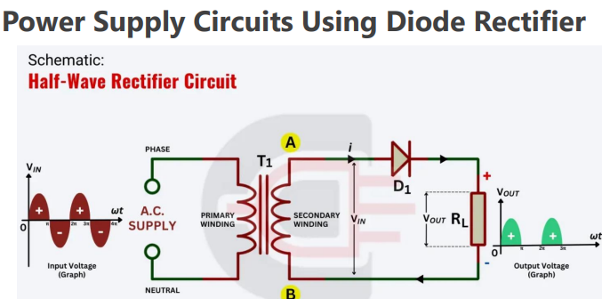
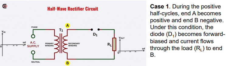
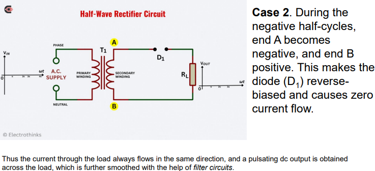
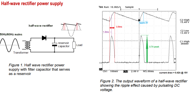
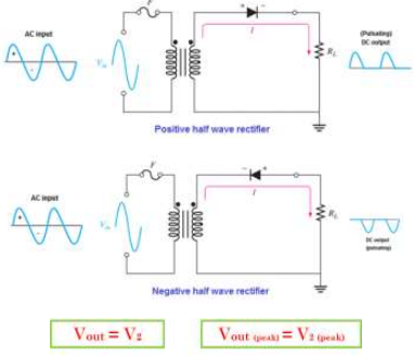
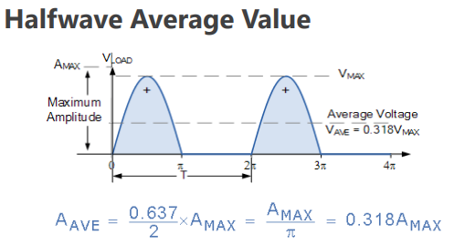
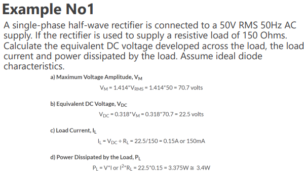
Half-Wave Rectifier
equivalent circuit of the half-wave rectifier with the diode replaced with its battery-plus-resistance model.
Transfer characteristics of the rectifier circuit.
Input and output waveforms.
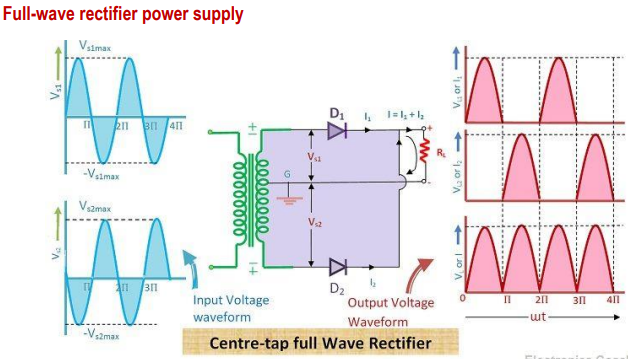
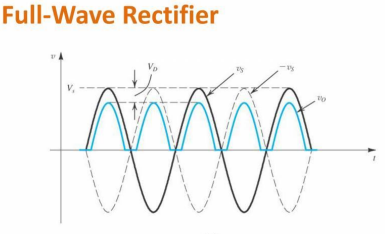
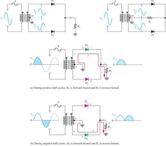
Full-Wave Rectifier
Transfer characteristics assuming a constant voltage-drop model for the diodes.
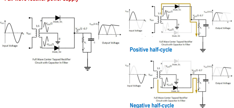
A center-tapped rectifier is a type of full-wave rectifier that uses two diodes connected to the secondary of a center-tapped transformer.
This is equivalent to 2 half wave rectifiers. Because of the center tap, each of these rectifiers has an input equal to half of the secondary voltage.
Input and output waveforms
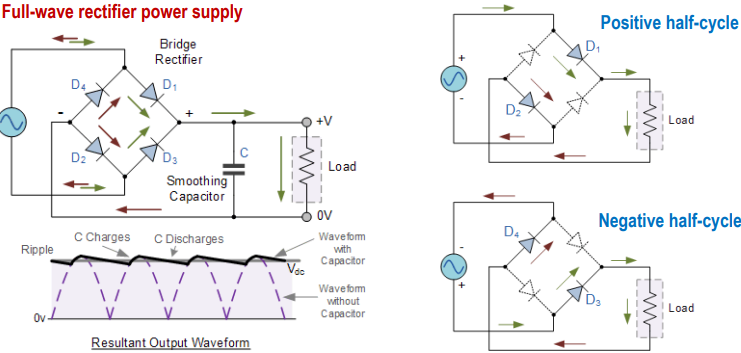
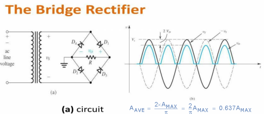
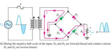
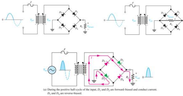
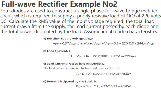
Bridge Rectifier
Input and output waveforms
Power Supply Circuit