Lecture 12
Digital Design using FPGAs
Lecture Overview
Topics Covered: FIFO and AXI4
Ready/Valid Interface - Submodule + Pipelining
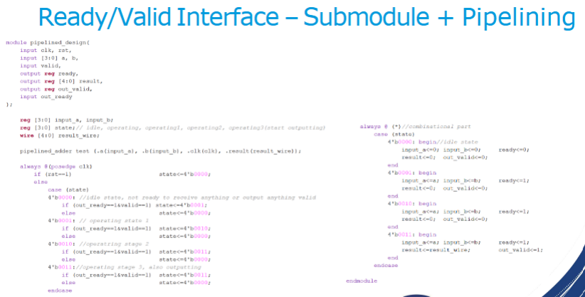
Module Definition
Module Name: pipelined_design
- This module is designed to create a pipelined architecture that allows for high throughput in data processing tasks by enabling multiple operations to occur in parallel across different pipeline stages.Inputs:
-clk: Clock signal, which synchronizes operation and ensures that internal states update according to the clock's rising edge. The frequency of this clock will impact the overall performance and throughput of the design.
-rst: Reset signal which initiates a system-wide reset to ensure that all registers and states are returned to a known state, essential for system initialization and fault recovery.
-a: A 4-bit input that represents one of the operands to the operation being performed by the design.
-b: Another 4-bit input serving as the second operand for the operation.
-valid: Valid input signal indicating when the inputsaandbare valid for processing, crucial for preventing erroneous operations when inputs are not ready.Outputs:
-ready: This output indicates readiness to process data. When 'ready' is asserted, it signals that the module can accept new inputs.
-result: A 5-bit result output representing the outcome of the operation (e.g., the sum or other computations) from the adder stage. The increase from 4 bits to 5 bits accommodates overflow.
-out_valid: Indicates the validity of the output result. This is crucial for downstream processing modules to know when the output can be safely used.Input:
-out_ready: An external input signal that indicates the readiness of the next module or component to receive the output. It is essential for ensuring smooth data flow and preventing data loss in scenarios where processing speeds may differ.
Internal Registers Definition
Registers:
-input_a: A 4-bit register used to store the value of inputaduring processing. This allows the module to hold the operand value across different clock cycles.
-input_b: A 4-bit register that stores the value of inputbsimilarly, ensuring data integrity throughout the operation stages.
-state: A 4-bit register that tracks the current state of the processing operation to facilitate the implementation of a finite state machine (FSM), detailing stages (idle, operation, etc.).Wire:
-result_wire: A 5-bit wire that carries the output result of the computation between stages within the module, allowing for proper connectivity to subsequent modules.
Instantiation of Pipelined Adder
Instantiation:
- Thepipelined_addermodule is instantiated with inputsinput_a,input_b, and the clock signalclk. The output of this instance feeds intoresult_wire, which represents the sum or result of the addition operation, effectively enabling parallel processing by separating the adder from other logics.
Main Control Logic
Always Block Triggered on Positive Clock Edge
Condition (Reset):
- If therstsignal is high, all operational states are reset to their initial values, ensuring that no erroneous data is processed and providing a clean slate for operation.State Machine Logic:
- State Transition Logic:
-0000: Idle state where the module is not ready to process any valid input or output, effectively idle and awaiting conditions to move to the next state.
- If bothout_readyandvalidinputs are high, the state transitions to0001, indicating readiness to process valid data.
- If not, remaining in state0000prevents processing errors.
- 0001: Operation stage 1, where the initial input validation occurs.
- As long as out_ready and valid remain high, the system continues in state 0001.
- Failure to meet conditions leads to either transitioning to 0010 or resetting back to 0000.
- 0010: Operation stage 2 where processing occurs, transitioning to 0011 as the processing approach aligns.
- 0011: Operation stage 3, where results are being output while still processing.
- If out_ready and valid are persistent, the state remains 0011.
- Failing these conditions leads back to 0000 to reset for another cycle.
Combinational Logic Block
Conditions Based on State
State
0000: Idle state
- Set all outputs and internal registers to zero, includinginput_a,input_b,result, andout_valid, ensuring no unexpected values are present.State
0001: Operation Initializing
- Setreadyto low, indicating the start of data processing.
- Assign inputs:input_a <= aandinput_b <= b, capturing current values for processing.
- Initializeresultandout_validto zero, while settingreadyto high, preparing for data flow.State
0010: Processing Data
- Input values are reassigned from a and b withinput_a <= aandinput_b <= b, maintaining a constant readiness state withreadyhigh and no valid output yet.State
0011: Output Phase
- Inputs are set withinput_a <= aandinput_b <= b, whilereadyindicates ongoing processing. The finalized result is outputted viaresult <= result_wire, andout_validis marked high to assert output availability.
FIFO Overview
FIFO (First-In, First-Out) is a queue where the first data that enters is also the first to leave. This structure is widely used for buffering data between different modules or systems in digital design.
FIFO States
Full State: The FIFO is said to be full when it cannot accept any more data. This condition occurs when the write pointer is at the maximum depth of the FIFO, meaning all storage locations are occupied.
- Implication: Attempting to write data when the FIFO is full leads to data loss or overwriting unless appropriate handshaking or flow control mechanisms are in place.Empty State: The FIFO is empty when there are no data items to read. This occurs when the read pointer catches up to the write pointer, indicating that all data has been processed.
- Implication: A read operation from an empty FIFO might return invalid data or require special handling to avoid errors.
Data Transfer Between Different Clock Domains
What if the write channel is faster than the read channel?
- Considerations: Data can overflow the FIFO, leading to data loss. To manage this, the FIFO must have enough depth to accommodate bursts until the read channel can catch up.What if the read channel is faster than the write channel?
- Considerations: The FIFO will eventually become empty, necessitating mechanisms to prevent unnecessary reads or handle empty conditions gracefully.Solution: Implementing proper FIFO depth can help buffer data during mismatches in transfer rates. Additionally, flow control signals should be utilized for synchronization between the channels.
FIFO Structure in FPGA
How Deep Should the FIFO Be? The required FIFO depth depends on the maximum data rates of the write and read channels, the expected burst sizes, and processing times. In practice, deeper FIFOs are preferable in high-speed designs.
FIFO Implementation Techniques in FPGA
Two Ways to Implement FIFO in FPGA:
1. Inference (Auto-detection by synthesis tool):
- Write RTL code following specific patterns.
- The synthesis tool detects patterns and infers the FIFO structure.
- Resources used include LUTs (SRL) and BRAM.
2. IP Instantiation (FIFO Generator):
- Use vendor-specific IP Catalog (e.g., Vivado FIFO Generator).
- Features customizable options including depth, width, dual-clock, and flags.
- Provides more control and flexibility in managing FIFO behavior.
Addressing Complex Point-to-Point FIFO Scenarios
Point-to-Point FIFO Problems:
- Resource Explosion: Each module may require multiple FIFOs leading to an increase in resource usage.
- Arbitration Logic: When multiple modules try to access the same FIFO resource simultaneously, additional logic may be required to manage access and prevent conflicts.Solution: Employ a Standard On-Chip Interconnect which includes built-in arbitration and flow control features to streamline connections among numerous modules.
AXI Protocol Overview
AMBA (Advanced Microcontroller Bus Architecture) is an open standard for on-chip interconnect protocols. The AXI (Advanced eXtensible Interface) targets communication between IP cores integrated in System-on-Chip (SoC) designs.
AXI Handshake Process
Basic Configuration: Connects two modules (Master and Slave). The Master initiates read/write requests, and the Slave responds accordingly.
Channels: - Write Address Channel (AW): Provides the address where data will be written. Includes signals AWVALID (from master) and AWREADY (from slave).
- Write Data Channel (W): Carries the data to be written. Signals include WVALID and WREADY.
- Write Response Channel (B): Indicates the status of the write operation. Signals include BVALID and BREADY.
- Read Address Channel (AR): Indicates the address from which data will be read. Signals include ARVALID and ARREADY.
- Read Data Channel (R): Transmits the actual read data. Signals include RVALID and RREADY.
AXI Features
AXI is optimized for FPGA implementations, separating address/control phases from data phases, allowing for flexible data transfers and burst-based transactions with a single issued start address.
Types of AXI
AXI4, AXI4-Lite, and AXI4-Stream:
- AXI4: Designed for high-bandwidth data transfers.
- AXI4-Lite: A simpler version supporting status monitoring.
- AXI4-Stream: Supports efficient data transfers in point-to-point configurations.